Page 111 - Sami Franssila Introduction to Microfabrication
P. 111
90 Introduction to Microfabrication


            7.10 EXERCISES                               Cote, D.R. et al: Low-temperature CVD processes and
                                                          dielectrics, IBM J. Res. Dev., 39 (1995), 437.
            1. The speed of sound in ZnO is 5700 m/s. What is the  Fang, W. & C.-Y. Lo: On the thermal expansion coefficients
               intended operating frequency for the TFBAR shown  of thin films, Sensors Actuators, 84 (2000), 310.
               in Figure 7.9?                            Guckel, H. et al: Fine-grained polysilicon films with build-in
            2. Calculate the wafer bow that a thin film of 100 nm  tensile strain, IEEE TED, 35 (1988), 800.
               thickness and 100 MPa stress induces on a 675 µm-  Hansen, M. & K. Anderko: Constitution of Binary Alloys, 2 nd
                                                          ed., McGraw-Hill, 1958.
               thick, 150 mm diameter silicon wafer. Also calculate
               the same for a 100 nm-thick film of 500 MPa stress  Hilleringmann, U. & K. Goser: Optoelectronic system inte-
                                                          gration on silicon: waveguides, photodetectors, and VLSI
               on a 380 µm-thick, 100 mm-diameter wafer?  CMOS circuits on one chip, IEEE TED, 42 (1995), 841.
            3. A periodic lattice of W and C is used as a λ/4 X-ray  Kang, U. et al: Pt/Ti thin film adhesion on SiN x /Si substrates,
               mirror. What are the layer thicknesses that should be  Jpn. J. Appl. Phys., 38 (1999), 4147.
               used for 100 eV X-rays?                   Laurila, T. et al: Failure mechanism of Ta diffusion barrier
            4. Oxygen is soluble into titanium up to 34 atomic%.  between Cu and Si, J. Appl. Phys., 88 (2000), 3377.
               What will be the thickness of a silicon dioxide film  Murarka, S.P.: Metallization, Theory and Practice for VLSI and
               that can be dissolved by a 50 nm-thick titanium film?  ULSI, Butterworth-Heinemann, 1993.
                                    3
               Titanium density is 4.5 g/cm , silicon dioxide density  Ohring, M.: The Materials Science of Thin Films, Academic
                       3
               is 2.3 g/cm .                              Press, 1992.
            5. What is the step coverage in Figures 7.15(b), 7.16(c),  Raaijmakers, I.J. et al: Microstructure and barrier properties
                                                          of reactively sputtered Ti-W nitride, J. Electron. Mater., 19
               and 7.19(a)?                               (1990), 1221.
            6. Draw the deposited film profile over a given topog-  Ritala, M. et al: Perfectly conformal TiN and Al 2 O 3 film
               raphy for the six different cases listed below:  deposited by atomic layer deposition, Chem. Vapor Deposit.,
              (a) Sputtered aluminium, 300 nm thick       5 (1999), 7.
              (b) CVD TEOS 0.3 µm thick                  Rossnagel, S.M. et al: Thin, high atomic weight refractory film
              (c) Electroplating 0.5 µm copper            deposition for diffusion barrier, adhesion layer and seed layer
              (d) PECVD oxide 0.2 µm thick                applications, J. Vac. Sci. Technol., B 14 (1996), 1819.
              (e) Evaporated aluminium, 100 nm thick     Smith, D.L.: Thin-film Deposition, McGraw-Hill, 1995.
                                                         Thornton, J.A.: The microstructure of sputter-deposited coat-
               (f) SOG application, 300 nm thick.
                                                          ings, J. Vac. Sci. Technol., A4(6) (1986), 3059.
                                                         Vallat-Sauvain, E. et al: Evolution of microstructure in micro-
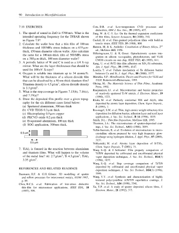
             0.5 µm                                       crystalline silicon prepared by very high frequency glow-
                                                          discharge using hydrogen dilution, J. Appl. Phys., 87 (2000),
                                                          3137.
                   0.5 µm                                Vehkam¨ aki, M. et al: Atomic layer deposition of SrTiO 3 ,
                                                          Chem. Vapor Deposit., 7 (2001), 75.
            7. TiAl 3 is formed in the reaction between aluminium  Wang, S.-Q. & J. Schlueter: Film property comparison of
               and titanium films. What will happen to the volume  Ti/TiN deposited by collimated and uncollimated physical
                                      3         3
               of the metal line? Al: 2.7 g/cm ; Ti 4.5 g/cm ; TiAl 3  vapor deposition techniques, J. Vac. Sci. Technol., B14(3)
                      3
               3.35 g/cm .                                (1996), 1837.
                                                         Wang, S.-Q. et al: Step coverage comparison of Ti/TiN
                                                          deposited by collimated and uncollimated physical vapor
            REFERENCES AND RELATED READINGS
                                                          deposition techniques, J. Vac. Sci. Technol., B14(3) (1996),
            Baumann, H.F. & G.H. Gilmer: 3D modelling of sputter  1846.
              and reflow processes for interconnect metals, IEDM 1995,  Wang, Y.Y. et al: Synthesis and characterization of highly
              p. 89.                                      textured polycrystalline AlN/TiN superlattice coatings, J.
            Chou, B.C.S. et al: Fabrication of low-stress dielectric  Vac. Sci. Technol., A16 (1998), 3341.
              thin-film for microsensor applications, IEEE EDL, 18  Xu, Y.P. et al: A study of sputter deposited silicon films, J.
              (1997), 599.                                Electron. Mater., 21 (1992), 373.

