
Page 116 - Sami Franssila Introduction to Microfabrication
P. 116
Pattern Generation 95
Electronic scan time and wafer stage mechanical 3. pattern processing resist development chrome etching
movement time must be considered for a com- (wet etching) resist stripping;
plete system 4. metrology CD (critical dimension) control;
τ 3 = A/Lv (8.4) 5. inspection for pattern integrity defects (in chrome)
pattern fidelity (shape and position);
where L is the electronic scan length and v is stage 6. cleaning particle removal, soft error reduction;
speed. 7. repair focused ion beam etching and/or deposition;
The time to write for a 10 cm × 10 cm area is 8. final defect inspection.
approximately one hour, as the calculations below show.
Typical resist sensitivities vary between 1 to 10 µC/cm 2 Adapted from Skinner, J.G. et al.
100 µC/cm 2 is usual for high-resolution resist, poly
methyl methacrylate (PMMA) and beam currents range Optical lithography can be done with reduction
from 1 to 250 nA (or even less for modified SEMs optical systems (to be discussed in the next chapter),
that are used as e-beam writers), which gives τ 1 of which means that the patterns on the mask are larger
the order of 400 to 40 000 s for 250 nA depending on than final structures on the wafer. This is a great relief
resist sensitivity. Write time τ 2 is, for example, 10 000 s for mask makers: 1 µm final size on a wafer corresponds
(0.1 µm pixel, 100 MHz). Assuming 250 µm electronic to 5 µm on the mask when 5X reduction optics is used.
scan length and 1 cm/s stage speed, τ 3 writing time
corresponds to 4000 s. Depending on resist selection,
either τ 1 or τ 2 gives the limiting write time. If highly 8.4 PHOTOMASKS AS TOOLS
sensitive resist is chosen, then pixel size sets the limit.
Photomasks are tools for process and device engineers
Photomasks with chrome-on-glass also go by the
(Figure 8.3). The process engineer wants to see the
name binary masks, because there is either a transmis-
resolution of the optical lithography process, and this is
sion or a blockade of light, but nothing else. In phase-
checked by linewidth test structures. Process robustness
shift masks, PSM, the phase of the light is manipulated
is tested by structures that span a range of values
while traversing the mask. PSMs will be discussed in
around the baseline process. For example, if the design
Chapter 38.
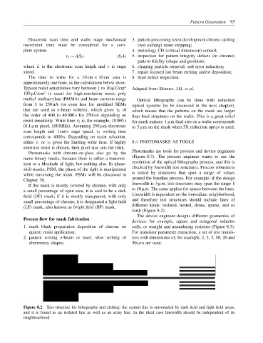
linewidth is 3 µm, test structures may span the range 1
If the mask is mostly covered by chrome, with only
to 10 µm. The same applies for spaces between the lines.
a small percentage of open area, it is said to be a dark
Linewidth is dependent on the immediate neighborhood,
field (DF) mask; if it is mostly transparent, with only
and therefore test structures should include lines of
small percentage of chrome, it is designated a light field
different kinds: isolated, nested, dense, sparse, and so
(LF) mask, also known as bright field (BF) mask.
forth (Figure 8.2).
The device engineer designs different geometries of
Process flow for mask fabrication
devices: for example, square and octagonal inductor
1. mask blank preparation deposition of chrome on coils, or straight and meandering resistors (Figure 8.3).
quartz; resist application; For transistor parameter extraction, a set of test transis-
2. pattern writing e-beam or laser; slow writing of tors with dimensions of, for example, 2, 3, 5, 10, 20 and
elementary shapes; 50 µm are used.
Figure 8.2 Test structure for lithography and etching: the central line is surrounded by dark field and light field areas,
and it is found as an isolated line as well as an array line. In the ideal case linewidth should be independent of its
neighbourhood