
Page 114 - Sami Franssila Introduction to Microfabrication
P. 114
8
Pattern Generation
A pattern generation tool transcribes the circuit design
data into a physical structure. It must be able to expose
single pixels and expose them fairly fast, since designs
can consist of millions of pixels. The first pattern
generators were optomechanical shutter systems with a Wafer
flash bulb. Aperture blades were sized and positioned,
followed by the exposing flash. After mechanical ~300 mm
movement of the wafer, the aperture sizing operation
and flashing was repeated, with operating frequency of
ca. 1 Hz. This method was employed in the early era of Stage
microfabrication when linewidths were above 10 µm. Chip scan
The most precise way of delineating structures is ~25 mm
by drawing a single feature with a focused beam
of electrons, ions or photons. This is faster than the
mechanical aperture method but still very slow. It has Main-field
three main applications: Beam
stepping
5 mm
1. Direct writing for ultimate resolution.
2. Direct writing in research and small series produc-
tion. Sub-field
3. Writing photomasks for optical lithography.
250 µm
Beam writing is several orders of magnitude slower
than optical lithography with photomasks but it offers
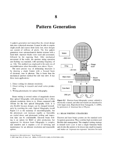
Figure 8.1 Electron beam lithography system: subfield is
ultimate resolution, down to ca. 10 nm compared with
electrically scanned, and other movements are introduced to
100 nm for the best optical lithography tools. It is
write larger areas. Reproduced from Yamaguchi, T. (2000),
also flexible because designs can be changed immedi-
by permission of American Inst of Physics
ately by rewriting the code. Optical lithography (recall
Figure 1.3) is the mainstay of microlithography, but
the photomask cost increases rapidly as linewidths 8.1 BEAM WRITING STRATEGIES
are scaled down, and photomask writing and inspec-
tion time can be considerable. Electron beam writ- Electron and laser beam systems are the standard tools
ing is an option for R&D or pilot production, but for pattern generation. They combine high resolution and
equipment for electron beam lithography is complex flexible data management. The simplest writing strategy
and sensitive and it requires a lot of servicing and is termed raster scan: it uses a single Gaussian beam
maintenance for an ultimate resolution and reasonable and divides the pattern to be drawn into small rectangles
uptime. and makes an ‘exposure-no-exposure’ decision for each
Introduction to Microfabrication Sami Franssila
2004 John Wiley & Sons, Ltd ISBNs: 0-470-85105-8 (HB); 0-470-85106-6 (PB)