
Page 117 - Sami Franssila Introduction to Microfabrication
P. 117
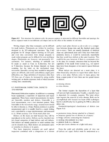
96 Introduction to Microfabrication


            Figure 8.3 Test structures for inductor coils: the process engineer is interested in different linewidths and spacings; the
            device engineer wants to test different coil shapes and see the effect of the number of coil turns


              Writing shapes other than rectangles can be difficult  perfect mask plate (known as die-to-die) or a compar-
            for mask makers. Photomasks are written by machines  ison between design data and the finished mask plate
            designed to do XY-orthogonal structures. The CAD  (die-to-data). There are usually hundreds of identical
            programs for IC design support drawing on XY-grid,  chips on a photomask plate and if they have been inde-
            and even data conversion from design program to  pendently drawn, it would be statistically improbable
            mask writer program can be difficult for non-rectilinear  that they would have defects at the same locations. This
            shapes. Photomasks are, however, not necessarily XY-  could be the case, however, if there is a systematic error
            symmetric. For instance, stitching of subfields can  in the data, for example, structures that are beyond the
            be made as small as 6 nm in X-direction, but not  capability of the mask writer system (e.g., too narrow
            in Y-direction, because the former depends on beam  lines have been designed, or too narrow spaces between
            scanning, but the latter on the mechanical stage  the lines).
            movement. Smoothly curving lines needed in integrated  When defects are detected on a mask plate, it is
            optics are difficult, and circles and arbitrary angles pose  often financially attractive to repair them rather than to
            difficulties, too. Edge definition of structures other than  write a new plate. Defects come in many guises, but
            XY-lines can, of course, be increased by using smaller  from a repair point of view there are two grand classes
            writing grid, or double exposure, both of which increase  of defects:
            writing time considerably.
                                                         • missing chrome
                                                         • extra chrome.
            8.5 PHOTOMASK INSPECTION, DEFECTS
            AND REPAIR
                                                           The former requires the deposition of a layer that
            Photomask fabrication requires, in addition to a scanning  will prevent light transmission. Usually, a metallic layer
            beam equipment, a repertoire of inspection and repair  is deposited, for example, tungsten. The latter defect
            equipment. Three basic control measurements for masks  type requires the removal of extra chrome. Both can be
            are linewidth, position and defects. Linewidth is a  accomplished with focused ion beam (FIB) techniques
            local measurement, over a test structure pattern. With  but the real difficulty lies in guiding the FIB to a detected
            linewidths in the micrometre range, measurement should  defect site.
            be able to discern ca. 10 nm. Pattern position is a global  Geometric/topological classification of defects (see
            measurement and it is usually fixed to a mask writing  Figure 8.4):
            tool, controlled by a stage interferometer, and measured
            to ca. 10 nm accuracy over 10 cm mask plate size.  • protrusion (extra chrome attached to a feature)
              Defects on the mask are fatal because they will be  • intrusion (partial loss of chrome in a feature)
            reproduced on the wafers. Defects can be classified into  • bridge (chrome connecting two features)
            two broad categories of hard defects and soft defects.  • necking (discontinuity in a line)
            Soft defects are mainly particles or resist residues that  • pinhole (hole in a chrome)
            can be cleaned away. Hard defects are permanent spots  • pin spot (extra chrome on a light field area).
            or scratches in chrome or in quartz.
              Two basic inspection strategies are used: optical  From the yield and reliability point of view not
            inspection combined with a comparison to a known  all defects are equal. Defect must be understood as a