
Page 121 - Sami Franssila Introduction to Microfabrication
P. 121
100 Introduction to Microfabrication
Sources of radiation
(UV 365 nm-436 nm,
DUV 193 nm-248 nm,
EUV, X-rays, electrons, ions)
Optical system I
(lenses, mirrors)
Mask (pattern)
Optical system II
(lenses, mirrors)
Numerical aperture a
NA=sin a
Imaging medium (resist)
Wafer (with patterns)
Wafer stage
(alignment mechanism)
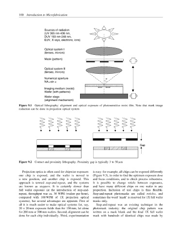
Figure 9.1 Optical lithography: alignment and optical exposure of photosensitive resist film. Note that mask image
reduction can be done in projection optical system
Gap
Figure 9.2 Contact and proximity lithography. Proximity gap is typically 3 to 50 µm
Projection optics is often used for chipwise exposure: is easy: for example, all chips can be exposed differently
one chip is exposed, and the wafer is moved to (Figure 9.3), in order to find the optimum exposure dose
a new position, and another chip is exposed. This and focus conditions, and to check process robustness.
approach is termed step-and-repeat, and the systems It is possible to change reticle between exposures,
are known as steppers. It is certainly slower than and have many different chips on one wafer in any
full wafer exposure (at the introduction of step-and- proportion. Inclusion of test chips is thus flexible.
repeat, throughput was ca. 30 WPH (wafers per hour), Step-and-repeat photomasks are called reticles, and
compared with 100 WPH of 1X projection optical sometimes the word ‘mask’ is reserved for 1X full wafer
systems), but several advantages are apparent. First of masks only.
all it is much easier to make optical systems for, say, Step-and-repeat was an existing technique in the
20 × 20 mm exposure fields than for 150 mm, let alone photomask industry: the original chip pattern was
for 200 mm or 300 mm wafers. Second, alignment can be written on a mask blank and the final 1X full wafer
done for each chip individually. Third, experimentation mask with hundreds of identical chips was made by