
Page 123 - Sami Franssila Introduction to Microfabrication
P. 123
102 Introduction to Microfabrication
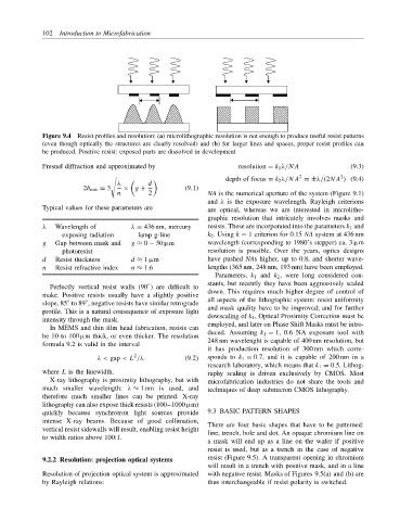
Figure 9.4 Resist profiles and resolution: (a) microlithographic resolution is not enough to produce useful resist patterns
(even though optically the structures are clearly resolved) and (b) for larger lines and spaces, proper resist profiles can
be produced. Positive resist: exposed parts are dissolved in development
Fresnel diffraction and approximated by resolution = k 1 λ/NA (9.3)
depth of focus = k 2 λ/NA = ±λ/(2NA ) (9.4)
2 2
λ d
2b min = 3 × g + (9.1)
n 2 NA is the numerical aperture of the system (Figure 9.1)
and λ is the exposure wavelength. Rayleigh criterions
Typical values for these parameters are are optical, whereas we are interested in microlitho-
graphic resolution that intricately involves masks and
λ Wavelength of λ = 436 nm, mercury resists. These are incorporated into the parameters k 1 and
exposing radiation lamp g-line k 2 . Using k = 1 criterion for 0.15 NA system at 436 nm
g Gap between mask and g ≈ 0 − 50 µm wavelength (corresponding to 1980’s stepper) ca. 3 µm
photoresist resolution is possible. Over the years, optics designs
d Resist thickness d ≈ 1 µm have pushed NAs higher, up to 0.8, and shorter wave-
n Resist refractive index n ≈ 1.6 lengths (365 nm, 248 nm, 193 nm) have been employed.
Parameters, k 1 and k 2 , were long considered con-
◦
Perfectly vertical resist walls (90 ) are difficult to stants, but recently they have been aggressively scaled
down. This requires much higher degree of control of
make. Positive resists usually have a slightly positive
◦
◦
slope, 85 to 89 , negative resists have similar retrograde all aspects of the lithographic system: resist uniformity
profile. This is a natural consequence of exposure light and mask quality have to be improved; and for further
intensity through the mask. dowscaling of k 1 , Optical Proximity Correction must be
In MEMS and thin film head fabrication, resists can employed, and later on Phase Shift Masks must be intro-
be 10 to 100 µm thick, or even thicker. The resolution duced. Assuming k 1 = 1, 0.6 NA exposure tool with
formula 9.2 is valid in the interval 248 nm wavelenght is capable of 400 nm resolution, but
it has production resolution of 300 nm which corre-
2
λ < gap < L /λ (9.2) sponds to k 1 = 0.7, and it is capable of 200 nm in a
research laboratory, which means that k 1 = 0.5. Lithog-
where L is the linewidth. raphy scaling is driven exclusively by CMOS. Most
X-ray lithography is proximity lithography, but with microfabrication industries do not share the tools and
much smaller wavelength: λ ≈ 1 nm is used, and techniques of deep submicron CMOS lithography.
therefore much smaller lines can be printed. X-ray
lithography can also expose thick resists (100–1000 µm)
quickly because synchrotron light sources provide 9.3 BASIC PATTERN SHAPES
intense X-ray beams. Because of good collimation, There are four basic shapes that have to be patterned:
vertical resist sidewalls will result, enabling resist height line, trench, hole and dot. An opaque chromium line on
to width ratios above 100:1.
a mask will end up as a line on the wafer if positive
resist is used, but as a trench in the case of negative
9.2.2 Resolution: projection optical systems resist (Figure 9.5). A transparent opening in chromium
will result in a trench with positive mask, and in a line
Resolution of projection optical system is approximated with negative resist. Masks of Figures 9.5(a) and (b) are
by Rayleigh relations: thus interchangeable if resist polarity is switched.