
Page 124 - Sami Franssila Introduction to Microfabrication
P. 124
Optical Lithography 103
(a) (b) (c) (d)
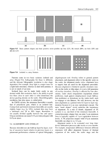
Figure 9.5 Basic pattern shapes and their positive resist profiles (a) line (LF); (b) trench (DF); (c) hole (DF) and
(d) dot (LF)
Figure 9.6 Isolated vs. array features
Patterns come in two basic varieties: isolated and align/exposure tool. Overlay refers to general pattern
array (Figure 9.6). Lithography for these is different, placement, and alignment refers to the specific spots on
and the ultimate lithographic resolution is also shape the wafer, the alignment marks (a.k.a. alignment keys
dependent. For example, stray light is a major issue for or targets) that are used for the alignment procedure.
a light field structures, whereas in dark field patterns, it Because alignment is limited to specific structures (usu-
is not so much of an issue. ally on the wafer or chip edge), it is not a full guarantee
Isolated lines can be made fairly easily in any of overlay elsewhere. Overlay is affected by lens aber-
desired width. But resolution, that is, the ability to print rations, wafer chuck irregularities (equipment related
two lines close to each other is what determines the problems), mask pattern misplacement (mask fabrica-
device-packing density on the wafer. Microlithographic tion problems) or distortions on the wafer itself, such
resolution, line plus space, is called pitch. as warpage or site flatness. We will, however, use the
In CMOS circuits, the minimum linewidth is usually term alignment as a general term for layer-to-layer reg-
that of polysilicon gate, which is an isolated line. istration because it is an easy operational concept. The
Contact hole and trench minimum linewidths are usually term “mask aligner” nicely underlies the importance
slightly larger (e.g. by 10%); isolated dots may have of alignment. As a rule of thumb, alignment of 1X
a minimum size 20 to 50% larger. Resolution is systems is ca. one-third of the minimum linewidth. A
not usually divided equally between line and space: contact/proximity aligner that can print 3 µm minimum
0.8 µm resolution can mean 0.35 µm wide polygate with lines is typically capable of 1 µm registration between
0.45 µm space. levels. A 5X projection stepper with 0.5 µm minimum
linewidth can align to ca. 0.1 µm.
Alignment needs to be evaluated over long time:
9.4 ALIGNMENT AND OVERLAY
device fabrication processes take weeks or even months.
Because microdevices are built-up layer-by-layer, over- For example, temperature differences between different
lay of successive layers relative to previous layers is a exposures will affect alignment because of thermal
paramount performance criterion of optical lithography expansion of the wafer, the wafer stage and the