
Page 125 - Sami Franssila Introduction to Microfabrication
P. 125
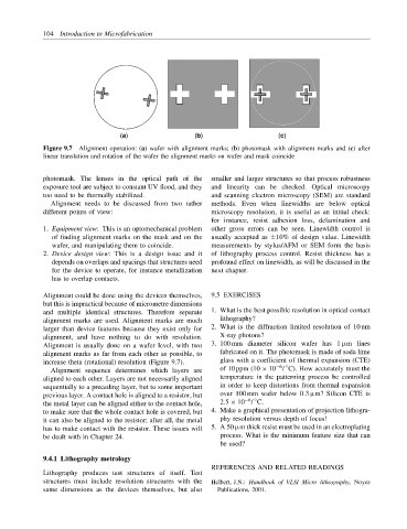
104 Introduction to Microfabrication


                                 (a)                (b)                   (c)
            Figure 9.7 Alignment operation: (a) wafer with alignment marks; (b) photomask with alignment marks and (c) after
            linear translation and rotation of the wafer the alignment marks on wafer and mask coincide


            photomask. The lenses in the optical path of the  smaller and larger structures so that process robustness
            exposure tool are subject to constant UV flood, and they  and linearity can be checked. Optical microscopy
            too need to be thermally stabilized.         and scanning electron microscopy (SEM) are standard
              Alignment needs to be discussed from two rather  methods. Even when linewidths are below optical
            different points of view:                    microscopy resolution, it is useful as an initial check:
                                                         for instance, resist adhesion loss, delamination and
            1. Equipment view: This is an optomechanical problem  other gross errors can be seen. Linewidth control is
               of finding alignment marks on the mask and on the  usually accepted as ±10% of design value. Linewidth
               wafer, and manipulating them to coincide.  measurements by stylus/AFM or SEM form the basis
            2. Device design view: This is a design issue and it  of lithography process control. Resist thickness has a
               depends on overlaps and spacings that structures need  profound effect on linewidth, as will be discussed in the
               for the device to operate, for instance metallization  next chapter.
               has to overlap contacts.

            Alignment could be done using the devices themselves,  9.5 EXERCISES
            but this is impractical because of micrometre dimensions
            and multiple identical structures. Therefore separate  1. What is the best possible resolution in optical contact
            alignment marks are used. Alignment marks are much  lithography?
            larger than device features because they exist only for  2. What is the diffraction limited resolution of 10 nm
            alignment, and have nothing to do with resolution.  X-ray photons?
            Alignment is usually done on a wafer level, with two  3. 100 mm diameter silicon wafer has 1 µm lines
            alignment marks as far from each other as possible, to  fabricated on it. The photomask is made of soda lime
            increase theta (rotational) resolution (Figure 9.7).  glass with a coefficient of thermal expansion (CTE)
                                                                          −6 ◦
              Alignment sequence determines which layers are  of 10 ppm (10 × 10 / C). How accurately must the
            aligned to each other. Layers are not necessarily aligned  temperature in the patterning process be controlled
            sequentially to a preceding layer, but to some important  in order to keep distortions from thermal expansion
            previous layer. A contact hole is aligned to a resistor, but  over 100 mm wafer below 0.3 µm? Silicon CTE is
                                                                 −6 ◦
            the metal layer can be aligned either to the contact hole,  2.5 × 10 / C.
            to make sure that the whole contact hole is covered, but  4. Make a graphical presentation of projection lithogra-
            it can also be aligned to the resistor; after all, the metal  phy resolution versus depth of focus!
            has to make contact with the resistor. These issues will  5. A 50 µm thick resist must be used in an electroplating
            be dealt with in Chapter 24.                   process. What is the minimum feature size that can
                                                           be used?

            9.4.1 Lithography metrology
                                                         REFERENCES AND RELATED READINGS
            Lithography produces test structures of itself. Test
            structures must include resolution structures with the  Helbert, J.N.: Handbook of VLSI Micro lithography, Noyes
            same dimensions as the devices themselves, but also  Publications, 2001.