
Page 122 - Sami Franssila Introduction to Microfabrication
P. 122
Optical Lithography 101
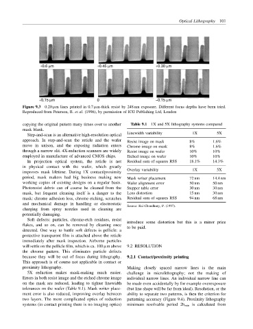
+0.6 µm +0.45 µm +0.30 µm
+0.15 µm 0 −0.15 µm
Figure 9.3 0.20 µm lines printed in 0.7 µm-thick resist by 248 nm exposure. Different focus depths have been tried.
Reproduced from Peterson, B. et al. (1996), by permission of ICG Publishing Ltd, London
copying the original pattern many times over to another Table 9.1 1X and 5X lithography systems compared
mask blank.
Linewidth variability 1X 5X
Step-and-scan is an alternative high-resolution optical
approach. In step-and-scan the reticle and the wafer Resist image on mask 8% 1.6%
move in unison, and the exposing radiation enters Chrome image on mask 8% 1.6%
through a narrow slit. 4X-reduction scanners are widely Resist image on wafer 10% 10%
employed in manufacture of advanced CMOS chips. Etched image on wafer 10% 10%
In projection optical system, the reticle is not Residual sum of squares RSS 18.1% 14.3%
in physical contact with the wafer, which greatly
improves mask lifetime. During 1X contact/proximity Overlay variability 1X 5X
period, mask makers had big business making new Mask writer placement 72 nm 14.4 nm
working copies of existing designs on a regular basis. Wafer alignment error 50 nm 50 nm
Photoresist debris can of course be cleaned from the Stepper table error 30 nm 30 nm
mask, but frequent cleaning itself is a danger to the Lens distortion 15 nm 30 nm
mask: chrome adhesion loss, chrome etching, scratches Residual sum of squares RSS 94 nm 68 nm
and mechanical damage in handling or electrostatic
Source: Rai-Choudhury, P. (1997).
charging from spray nozzles used in cleaning are
potentially damaging.
Soft defects: particles, chrome-etch residues, resist introduce some distortion but this is a minor price
flakes, and so on, can be removed by cleaning once to be paid.
detected. One way to battle soft defects is pellicle: a
protective transparent film is attached above the reticle
immediately after mask inspection. Airborne particles
will settle on the pellicle film, which is ca. 100 µm above 9.2 RESOLUTION
the chrome pattern. This eliminates particle defects
because they will be out of focus during lithography. 9.2.1 Contact/proximity printing
This approach is of course not applicable in contact or
proximity lithography. Making closely spaced narrow lines is the main
5X reduction makes mask-making much easier. challenge in microlithography; not the making of
Errors in both resist image and the etched chrome image individual narrow lines. An individual narrow line can
on the mask are reduced, leading to tighter linewidth be made even accidentally by for example overexposure
tolerances on the wafer (Table 9.1). Mask writer place- (but line shape will be far from ideal). Resolution, or the
ment error is also reduced, improving overlay between ability to separate two patterns, is then the criterion for
two layers. The more complicated optics of reduction patterning accuracy (Figure 9.4). Proximity lithography
systems (in contact printing there is no imaging optics) minimum resolvable period 2b min is calculated from