
Page 118 - Sami Franssila Introduction to Microfabrication
P. 118
Pattern Generation 97
incrementing rate is 500 MHz and mask plate area
8 cm × 8 cm? The photomask is 4X the final size.
4. What process and materials parameters do you need
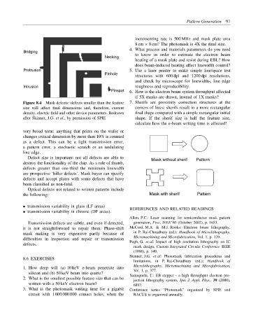
Bridging
Necking to know in order to estimate the electron beam
heating of a mask plate and resist during EBL? How
does beam-induced heating affect linewidth control?
Protrusion 5. Use a laser printer to make simple line/space test
Pinhole
structures with 600 dpi and 1200 dpi resolutions,
and check by microscope for linewidths, line edge
Intrusion roughness and reproducibility.
Pinspot 6. How is the electron beam system throughput affected
if 5X masks are drawn, instead of 1X masks?
Figure 8.4 Mask defects: defects smaller than the feature 7. Sherifs are proximity correction structures at the
size will affect final dimensions and, therefore, current corners of lines: sherifs result in a more rectangular
density, electric field and other device parameters. Redrawn final shape compared with a simple rectangular initial
after Skinner, J.G. et al., by permission of SPIE shape. If the sherif size is half the feature size,
calculate how the e-beam writing time is affected!
very broad term: anything that prints on the wafer or
changes critical dimension by more than 10% is counted
as a defect. This can be a light transmission error,
a pattern error, a stochastic scratch or an undulating
line edge.
Defect size is important: not all defects are able to Mask without sherif Pattern
destroy the functionality of the chip. As a rule of thumb,
defects greater than one-third the minimum linewidth
are prospective ‘killer defects’. Mask buyer can specify
defects and accept plates with some defects that have
been classified as non-fatal.
Optical defects not related to written patterns include
the following: Mask with sherif Pattern
• transmission variability in glass (LF areas)
REFERENCES AND RELATED READINGS
• transmission variability in chrome (DF areas).
Allen, P.C.: Laser scanning for semiconductor mask pattern
Transmission defects are subtle, and even if detected, generation, Proc. IEEE’90 (October 2002), p. 1653.
it is not straightforward to repair them. Phase-shift McCord, M.A. & M.J. Rooks: Electron beam lithography,
mask making is very expensive partly because of in P. Rai-Choudhury (ed.): Handbook of Microlithography,
difficulties in inspection and repair or transmission Micromachining and Microfabrication, Vol. 1, p. 139.
defects. Pugh, G. et al: Impact of high resolution lithography on IC
mask design, Custom Integrated Circuits Conference IEEE
(1998), p. 149.
Skinner, J.G. et al: Photomask fabrication procedures and
8.6 EXERCISES
limitations, in P. Rai-Choudhury (ed.): Handbook of
Microlithography, Micromachining and Microfabrication,
1. How deep will (a) 10 keV e-beam penetrate into Vol. 1, p. 377.
silicon and (b) 50 keV beam into quartz? Yamaguchi, T.: EB stepper – a high throughput electron pro-
2. What is the smallest possible feature size that can be jection lithography system, Jpn. J. Appl. Phys., 39 (2000),
written with a 50 keV electron beam? 6897.
3. What is the photomask writing time for a gigabit Conference series “Photomask” organized by SPIE and
circuit with 1 000 000 000 contact holes, when the BACUS is organized annually.