
Page 129 - Sami Franssila Introduction to Microfabrication
P. 129
108 Introduction to Microfabrication
and if the film is not dry, it will flow on an uneven
surface after spin coating. It is also possible to apply
a thick resist by multiple coatings of thinner layers.
Soft baking for solvent removal must be done after each
application.
10.1.2 Edge bead
(a) Spin-film definition at the wafer edge is often poor:
the resist always flows over the edge, but the film at
the edge is discontinuous or non-uniform. Some film is
easily transported to the back of the wafer, which may
cause contamination in subsequent process steps. Drying
during spinning increases viscosity at the edges, which
causes accumulation of material on the rim of the wafer.
This is known as edge bead.
Edge bead removal (EBR) is a process in which a
directed solvent jet etches the resist away from the wafer
edges. This does not diminish the number of usable
(b)
chips because the edge chips are usually non-functional
anyway. The opposite of EBR is sometimes used in
MEMS: in order to prevent edge chipping during long
wet etching, edges are protected by extra resist.
10.2 RESIST CHEMISTRY
Resists have three main components:
(c)
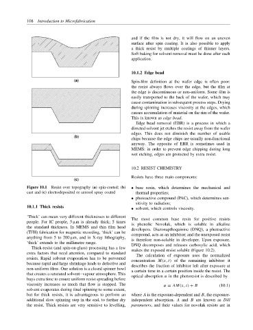
Figure 10.1 Resist over topography (a) spin-coated; (b) • base resin, which determines the mechanical and
cast and (c) electrodeposited or aerosol spray coated thermal properties;
• photoactive compound (PAC), which determines sen-
sitivity to radiation;
10.1.1 Thick resists
• solvent, which controls viscosity.
‘Thick’ can mean very different thicknesses to different The most common base resin for positive resists
people. For IC people, 5 µm is already thick; 5 times is phenolic Novolak, which is soluble in alkaline
the standard thickness. In MEMS and thin film head developers. Diazonapthoquinine (DNQ), a photoactive
(TFH) fabrication for magnetic recording, ‘thick’ can be compound, acts as an inhibitor; and the unexposed resist
anything from 5 to 200 µm, and in X-ray lithography, is therefore non-soluble in developer. Upon exposure,
‘thick’ extends to the millimetre range. DNQ decomposes and releases carboxylic acid, which
Thick-resist (and spin-on-glass) processing has a few makes the exposed resist soluble (Figure 10.2).
extra factors that need attention, compared to standard The calculation of exposure uses the normalized
resists. Rapid solvent evaporation has to be prevented concentration M(x, t) of the remaining inhibitor: it
because rapid and large shrinkage leads to defective and describes the fraction of inhibitor left after exposure at
non-uniform films. One solution is a closed spinner bowl a certain time in a certain position inside the resist. The
that creates a saturated solvent–vapour atmosphere. This optical absorption α in the photoresist is described by
buys extra time to ensure uniform resist spreading before
viscosity increases so much that flow is stopped. The α = AM(x, t) + B (10.1)
solvent evaporates during final spinning to some extent,
but for thick resists, it is advantageous to perform an where A is the exposure-dependent and B, the exposure-
additional slow spinning step in the end, to further dry independent absorption. A and B are known as Dill
the resist. Thick resists are very sensitive to levelling, parameters, and their values for novolak resists are in