
Page 131 - Sami Franssila Introduction to Microfabrication
P. 131
110 Introduction to Microfabrication
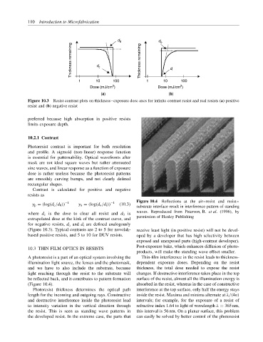
d 0 d o
Thickness remaining d c Thickness remaining d i
1 10 100 1 10 100
2
2
Dose (mJ/cm ) Dose (mJ/cm )
(a) (b)
Figure 10.3 Resist contrast plots on thickness–exposure dose axes for infinite contrast resist and real resists (a) positive
resist and (b) negative resist
preferred because high absorption in positive resists
limits exposure depth.
10.2.1 Contrast
Photoresist contrast is important for both resolution
and profile. A sigmoid (non-linear) response function
is essential for patternability. Optical wavefronts after
mask are not ideal square waves but rather attenuated
sine waves, and linear response as a function of exposure
dose is rather useless because the photoresist patterns
are smoothly curving bumps, and not clearly defined
rectangular shapes.
Contrast is calculated for positive and negative
resists as
Figure 10.4 Reflections at the air–resist and resist–
−1
−1
γ p = (log(d c /d 0 )) γ n = (log(d o /d i )) (10.3)
substrate interface result in interference pattern of standing
waves. Reproduced from Peterson, B. et al. (1996), by
where d c is the dose to clear all resist and d 0 is
permission of Henley Publishing
extrapolated dose at the kink of the contrast curve, and
for negative resists, d o and d i are defined analogously
(Figure 10.3). Typical contrasts are 2 to 5 for novolak- receive least light (in positive resist) will not be devel-
based positive resists, and 5 to 10 for DUV resists. oped by a developer that has high selectivity between
exposed and unexposed parts (high-contrast developer).
Post-exposure bake, which enhances diffusion of photo-
10.3 THIN FILM OPTICS IN RESISTS
products, will make the standing wave effect smaller.
A photoresist is a part of an optical system involving the Thin-film interference in the resist leads to thickness-
illumination light source, the lenses and the photomask, dependent exposure doses. Depending on the resist
and we have to also include the substrate, because thickness, the total dose needed to expose the resist
light reaching through the resist to the substrate will changes. If destructive interference takes place in the top
be reflected back, and it contributes to pattern formation surface of the resist, almost all the illumination energy is
(Figure 10.4). absorbed in the resist, whereas in the case of constructive
Photoresist thickness determines the optical path interference at the top surface, only half the energy stays
length for the incoming and outgoing rays. Constructive inside the resist. Maxima and minima alternate at λ/(4n)
and destructive interference inside the photoresist lead intervals; for example, for the exposure of a resist of
to intensity variation in the vertical direction through refractive index 1.64 to light of wavelength λ = 365 nm,
the resist. This is seen as standing wave patterns in this interval is 56 nm. On a planar surface, this problem
the developed resist. In the extreme case, the parts that can easily be solved by better control of the photoresist