
Page 134 - Sami Franssila Introduction to Microfabrication
P. 134
Lithographic Patterns 113
reacts with the resist during baking, and forms a non-
soluble layer on the sidewalls of the contact hole,
making the hole smaller (should there be photoresist
residue at the bottom, it would block the contact hole).
0.25 µm contact holes have been reduced to 0.10 µm
with this method.
10.5 LITHOGRAPHY SIMULATION
Figure 10.8 Resist trimming: resist lines made narrower
by isotropic etching of the resist in oxygen plasma. The lithographic pattern formation starts with the
Resolution (line + space) remains constant
designer’s layout file, which is turned into a physical
mask plate in a mask shop. This mask is inserted into the
photoresist is then performed (Figure 10.8). Resist line exposure tool, where it modifies the illumination from
gets narrower and thinner. This method is most suitable the light source. After complex photochemistry steps
when reasonably narrow lines can be used as starting in the photoresist, development creates patterns in the
point. Lines of 1.0 µm original width and thickness can resist (Figure 10.10). This information flow has many
be narrowed down to 0.2 µm; a 0.4 µm horizontal nar- points where errors can occur, and where dimensions
rowing from both sides. Resist thickness after thinning is are not accurately transferred. Some of these are data
0.6 µm because isotropic thinning was employed. This errors related to formats used in drawing and mask
is a useful approach for studying simple structures, such writing, and some are physical, and related to both
as individual lines of scaled-down dimensions. Small mask writing and exposure resolution, and to etching
MOSFETs of ca. 20 nm gate lengths have been made by tolerances.
resist trimming by using a 200 nm initial linewidth. But It should be noted that the mask writing process has
line plus space remains intact, and no more devices can a similar information flow and similar error sources: the
be made to fit on a wafer. mask writer has finite resolution, the photoresist used
in mask writing is similar to resists used in optical
lithography, and chrome etching has its non-idealities
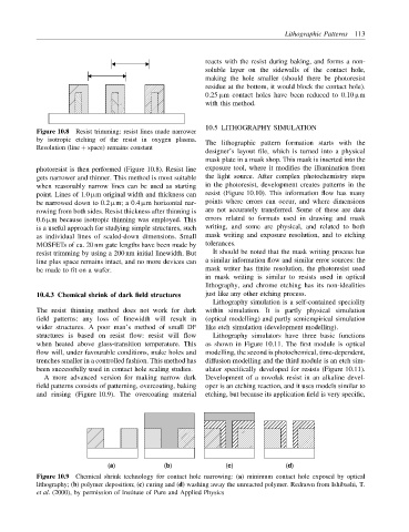
10.4.3 Chemical shrink of dark field structures just like any other etching process.
Lithography simulation is a self-contained speciality
The resist thinning method does not work for dark within simulation. It is partly physical simulation
field patterns: any loss of linewidth will result in (optical modelling) and partly semiempirical simulation
wider structures. A poor man’s method of small DF like etch simulation (development modelling).
structures is based on resist flow: resist will flow Lithography simulators have three basic functions
when heated above glass-transition temperature. This as shown in Figure 10.11. The first module is optical
flow will, under favourable conditions, make holes and modelling, the second is photochemical, time-dependent,
trenches smaller in a controlled fashion. This method has diffusion modelling and the third module is an etch sim-
been successfully used in contact hole scaling studies. ulator specifically developed for resists (Figure 10.11).
A more advanced version for making narrow dark Development of a novolak resist in an alkaline devel-
field patterns consists of patterning, overcoating, baking oper is an etching reaction, and it uses models similar to
and rinsing (Figure 10.9). The overcoating material etching, but because its application field is very specific,
(a) (b) (c) (d)
Figure 10.9 Chemical shrink technology for contact hole narrowing: (a) minimum contact hole exposed by optical
lithography; (b) polymer deposition; (c) curing and (d) washing away the unreacted polymer. Redrawn from Ishibashi, T.
et al. (2000), by permission of Institute of Pure and Applied Physics