
Page 135 - Sami Franssila Introduction to Microfabrication
P. 135
114 Introduction to Microfabrication
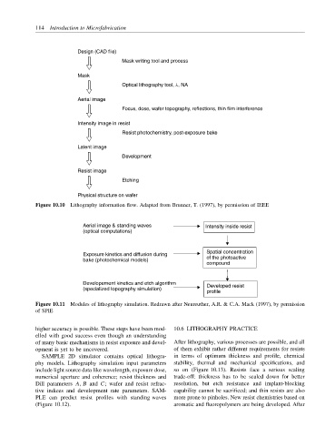
Design (CAD file)
Mask writing tool and process
Mask
Optical lithography tool, l, NA
Aerial image
Focus, dose, wafer topography, reflections, thin film interference
Intensity image in resist
Resist photochemistry, post-exposure bake
Latent image
Development
Resist image
Etching
Physical structure on wafer
Figure 10.10 Lithography information flow. Adapted from Brunner, T. (1997), by permission of IEEE
Aerial image & standing waves Intensity inside resist
(optical computations)
Spatial concentration
Exposure kinetics and diffusion during
bake (photochemical models) of the photoactive
compound
Developement kinetics and etch algorithm Developed resist
(specialized topography simulation)
profile
Figure 10.11 Modules of lithography simulation. Redrawn after Neureuther, A.R. & C.A. Mack (1997), by permission
of SPIE
higher accuracy is possible. These steps have been mod- 10.6 LITHOGRAPHY PRACTICE
elled with good success even though an understanding
of many basic mechanisms in resist exposure and devel- After lithography, various processes are possible, and all
opment is yet to be uncovered. of them exhibit rather different requirements for resists
SAMPLE 2D simulator contains optical lithogra- in terms of optimum thickness and profile, chemical
phy models. Lithography simulation input parameters stability, thermal and mechanical specifications, and
include light source data like wavelength, exposure dose, so on (Figure 10.13). Resists face a serious scaling
numerical aperture and coherence; resist thickness and trade-off: thickness has to be scaled down for better
Dill parameters A, B and C; wafer and resist refrac- resolution, but etch resistance and implant-blocking
tive indices and development rate parameters. SAM- capability cannot be sacrificed; and thin resists are also
PLE can predict resist profiles with standing waves more prone to pinholes. New resist chemistries based on
(Figure 10.12). aromatic and fluoropolymers are being developed. After