Page 136 - Sami Franssila Introduction to Microfabrication
P. 136

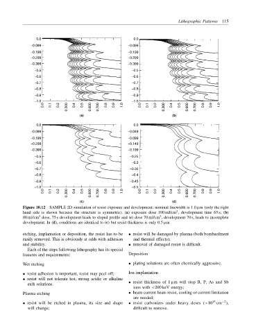
Lithographic Patterns 115


                0.0                                      0.0
              −0.099                                   −0.099
              −0.199                                   −0.199
              −0.299                                   −0.299
              −0.399                                   −0.399
               −0.5                                     −0.5
               −0.6                                     −0.6
               −0.7                                     −0.7
               −0.8                                     −0.8
               −0.9                                     −0.9
               −1.0                                     −1.0
                   0.0  0.1  0.2  0.300  0.4  0.5  0.600  0.700  0.8  0.9  1.0  0.0  0.1  0.2  0.300  0.4  0.5  0.600  0.700  0.8  0.9  1.0

                                  (a)                                    (b)
                0.0                                      0.0
              −0.099                                   −0.049
              −0.199                                   −0.099
              −0.299                                   −0.149
              −0.399                                   −0.199
               −0.5                                    −0.25
               −0.6                                     −0.3
               −0.7                                    −0.35
               −0.8                                     −0.4
               −0.9                                    −0.45
               −1.0                                     −0.5
                   0.0  0.1  0.2  0.300  0.4  0.5  0.600  0.700  0.8  0.9  1.0  0.0  0.1  0.2  0.300  0.4  0.5  0.600  0.700  0.8  0.9  1.0

                                  (c)                                    (d)
           Figure 10.12 SAMPLE 2D simulation of resist exposure and development: nominal linewidth is 1.0 µm (only the right
                                                                           2
           hand side is shown because the structure is symmetric). (a) exposure dose 100 mJ/cm , development time 65 s; (b)
                 2
                                                                    2
           80 mJ/cm dose, 75 s development leads to sloped profile and (c) dose 70 mJ/cm , development 70 s, leads to incomplete
           development. In (d), conditions are identical to (c) but resist thickness is only 0.5 µm
           etching, implantation or deposition, the resist has to be  • resist will be damaged by plasma (both bombardment
           easily removed. This is obviously at odds with adhesion  and thermal effects);
           and stability.                              • removal of damaged resist is difficult.
             Each of the steps following lithography has its special
           features and requirements:                  Deposition

           Wet etching                                 • plating solutions are often chemically aggressive.
           • resist adhesion is important, resist may peel off;  Ion implantation
           • resist will not tolerate hot, strong acidic or alkaline
             etch solutions.                           • resist thickness of 1 µm will stop B, P, As and Sb
                                                         ions with <200 keV energy;
           Plasma etching                              • beam current heats resist, cooling or current limitation
                                                         are needed;
                                                                                              −2
                                                                                          15
           • resist will be etched in plasma, its size and shape  • resist carbonizes under heavy doses (>10 cm ),
             will change;                                difficult to remove.
   131   132   133   134   135   136   137   138   139   140   141