
Page 133 - Sami Franssila Introduction to Microfabrication
P. 133
112 Introduction to Microfabrication
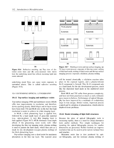
Thick polymer
Substrate Substrate
(a)
Substrate Substrate
Substrate Substrate
(a) (b)
(b) Figure 10.7 Multilayer resist and top-surface imaging. (a)
Figure 10.6 Reflective notching. (a) Top view of dis- Tri-layer resist process: exposure of thin top resist; etching
torted resist lines and (b) cross-sectional view shows of thin hard mask; etching of thick resist and (b) top-surface
how the underlying metal line reflects incoming light into imaging process: exposure; silylation; plasma etching
resist sidewall
will be treated chemically: a silylation reaction takes
underlying metal lines can cause resist exposure in place in the exposed regions, and a plasma-tolerant
unwanted places. This is called reflective notching Si–O compound is formed. This Si–O compound acts
(Figure 10.6). as a hard mask for the dry development process, much
like the deposited hard mask in the multilevel resist
process.
10.4 EXTENDING OPTICAL LITHOGRAPHY Both MLR and TSI suffer from process complexity,
and have not been practised as much as early estimates
10.4.1 Top-surface imaging and multilayer resists gave reason to believe. Performance of optical lithogra-
phy has been improved by a multitude of evolutionary
Top-surface imaging (TSI) and multilayer resists (MLR) steps in lens design, thinner resists, improved process
offer true improvements in resolution, and therefore, control and by adoption of planarization, which relieves
device-packing density. Both bilayer and tri-layer resists depth-of-focus problems.
have been tried. TSI and MLR rely on the fact that high
resolution is easier to achieve in a thin imaging layer.
In MLR, a thick planarizing layer is applied first, 10.4.2 Resist trimming of light field structures
followed by a hard mask layer of glass-like material
(e.g., spin-on-glass). A very thin imaging layer is Because the price of optical lithography tools is
then applied (Figure 10.7). MLR eliminates focus depth increasing rapidly, there is a need for cheap alternative
effects if the planarizing resist works well. After tools and/or methods. Two simple techniques for
developing the thin top imaging resist, plasma etching tweaking the optical lithography process for smaller
is used to pattern the hard mask, which then acts as a dimensions are presented. Neither method can improve
mask for dry development (oxygen plasma etching) of resolution but can be used to print narrow isolated lines
the thick planarizing layer. and trenches.
Top-surface imaging uses a dyed resist for maximum Minimum resist line is first produced by opti-
absorption in the thin top layer. The exposed areas cal lithography, and the isotropic plasma etching of