
Page 110 - Sami Franssila Introduction to Microfabrication
P. 110
Thin-film Growth and Structure 89
0.0 0.0
−0.194 −0.194
−0.388 −0.388
−0.582 −0.582
−0.776 −0.776
−0.970 −0.970
−1.164 −1.164
−1.358 −1.358
−1.552 −1.552
−1.746 −1.746
−1.940 −1.940
0.0 0.306 0.613 0.920 1.227 1.534 1.841 2.148 2.455 2.762 3.069 0.0 0.306 0.613 0.920 1.227 1.534 1.841 2.148 2.455 2.762 3.069
(a) (b)
0.0
−0.194
−0.388
−0.582
−0.776
−0.970
−1.164
−1.358
−1.552
−1.746
−1.940
0.0 0.306 0.613 0.920 1.227 1.534 1.841 2.148 2.455 2.762 3.069
(c)
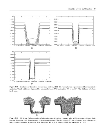
Figure 7.18 Simulation of deposition step coverage with SAMPLE 2D. Hemispherical deposition model corresponds to
sputtering. Trench widths are 1 µm and 0.5 µm, depths 1 µm. Wall angle either 90 or ca. 81 . Film thickness is 0.5 µm
◦
◦
in all cases
(a) (b)
Figure 7.19 3D Monte Carlo simulation of aluminium deposition into a contact hole: (a) high-rate deposition and (b)
low-rate deposition. Both depositions are at the same temperature. The simulation is 3D, but only a cut through the contact
hole centreline is shown. Reproduced from Baumann, H.F. & G.H. Gilmer (1995), by permission of IEEE