
Page 105 - Sami Franssila Introduction to Microfabrication
P. 105
84 Introduction to Microfabrication
temperatures, but the situation is really much more Mo
complex because stress relaxation can occur during high- Tension Cr Ta
temperature deposition.
The coefficient of thermal expansion (CTE) of silicon Pt
−6 ◦
is 2.6 × 10 / C (around room temperature). The only
other materials used in microfabrication that have
smaller coefficients are silicon dioxide, silicon nitride
−6 ◦
and diamond which have CTEs 0.5 × 10 / C, 2.4 ×
−6 ◦
−6 ◦
10 / C and 1.1 × 10 / C, respectively. Oxide, nitride Compression
and diamond, are therefore the only materials that
can develop compressive extrinsic stresses over silicon 0.1 Pa 1 Pa
substrates. Aluminium CTE is 23 ppm, which is fairly Pressure
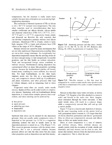
high, tungsten CTE is 4 ppm and polymers have CTE Figure 7.11 Sputtering pressure and film stress. Atomic
values in the range of 30 to 100 ppm. masses: Cr 52, Mo 96, Ta 181, Pt 195. Redrawn after
Intrinsic stresses are caused by many mechanisms that Ohring, M. (1992), by permission of Academic Press
are not fully understood. Deposited polycrystalline films
are not at their energy minimum. An exceptionally low
deposition temperature means that the arriving atoms do
not have enough energy to find energetically favourable
positions, and the film builds up without relaxation.
Voids and incorporated foreign atoms contribute to
intrinsic stresses. Bombardment during deposition has
a pronounced effect on many film properties, including
stresses, because the bombardment pinches off loosely
bound atoms, resulting in a more uniform, less stressed
film. Too high bombardment, on the other hand, Tensile stress Compressive stress
(negative)
implants atoms into the film in a non-equilibrium (positive)
(a) (b)
way, and compressive stresses build up. Crystallization
and phase transitions, and other processes that lead Figure 7.12 Thin-film stresses: a film that must be
to volume changes, such as outgassing, lead to stress elongated to fit a wafer is under tensile stress (positive) and
changes. a film that is compressed to fit a wafer, is under compressive
(negative) stress
Evaporated metal films are usually under tensile
stresses. Sputtered films can be under tensile or compres-
sive stresses. Sputtering, with ion bombardment during
Stresses in thin films cause wafer curvature, as shown
deposition, is a much more complex process than evap-
in Figure 7.12. Imagine a free film attached to a massive
oration, and stress tailoring can be achieved by:
wafer and forcefit to the wafer size. Next, imagine,
stress relaxation through the wafer curvature. A film
• bias power under tensile stress will result in a concave shape,
• argon pressure while a compressively stressed film will end up with
• sputtering gas mass a convex profile.
• temperature Figure 7.12 gives a macroscopic depiction of stresses,
• deposition rate. but the same reasoning works on the atomic level as
well: germanium lattice constant is 4.2% larger than that
Sputtered film stress can be tailored by the deposition of silicon, therefore germanium and silicon–germanium
pressure: films are usually under compressive stress if films on silicon are compressively stressed, and silicon
deposited at low pressure (ca. 0.1 Pa in a magnetron films on SiGe are under tensile stress.
sputtering system) but turn to tensile stress as the Stress at room temperature is a sum of intrinsic
deposition pressure is raised (to ca. 1 Pa) (Figure 7.11). and extrinsic stresses. Since extrinsic stresses are
This crossover pressure increases with the atomic mass. usually tensile (with the exception of oxide, nitride and
However, this is not a universal solution, because diamond), and total stresses can be close to zero, this
pressure affects not only the film stress but also many means that intrinsic stresses from the deposition process
other properties such as deposition rate and film density. are compressive. This is often the case.