
Page 100 - Sami Franssila Introduction to Microfabrication
P. 100
Thin-film Growth and Structure 79
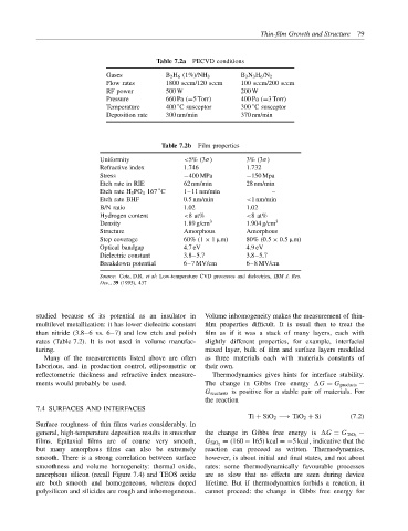
Table 7.2a PECVD conditions
Gases B 2 H 6 (1%)/NH 3 B 3 N 3 H 6 /N 2
Flow rates 1800 sccm/120 sccm 100 sccm/200 sccm
RF power 500 W 200 W
Pressure 660 Pa (=5 Torr) 400 Pa (=3 Torr)
◦
◦
Temperature 400 C susceptor 300 C susceptor
Deposition rate 300 nm/min 370 nm/min
Table 7.2b Film properties
Uniformity <5% (3σ) 3% (3σ)
Refractive index 1.746 1.732
Stress −400 MPa −150 Mpa
Etch rate in RIE 62 nm/min 28 nm/min
◦
Etch rate H 3 PO 4 167 C 1–11 nm/min –
Etch rate BHF 0.5 nm/min <1 nm/min
B/N ratio 1.02 1.02
Hydrogen content <8 at% <8 at%
Density 1.89 g/cm 3 1.904 g/cm 3
Structure Amorphous Amorphous
Step coverage 60% (1 × 1 µm) 80% (0.5 × 0.5 µm)
Optical bandgap 4.7 eV 4.9 eV
Dielectric constant 3.8–5.7 3.8–5.7
Breakdown potential 6–7 MV/cm 6–8 MV/cm
Source: Cote, D.R. et al: Low-temperature CVD processes and dielectrics, IBM J. Res.
Dev., 39 (1995), 437
studied because of its potential as an insulator in Volume inhomogeneity makes the measurement of thin-
multilevel metallization: it has lower dielectric constant film properties difficult. It is usual then to treat the
than nitride (3.8–6 vs. 6–7) and low etch and polish film as if it was a stack of many layers, each with
rates (Table 7.2). It is not used in volume manufac- slightly different properties, for example, interfacial
turing. mixed layer, bulk of film and surface layers modelled
Many of the measurements listed above are often as three materials each with materials constants of
laborious, and in production control, ellipsometric or their own.
reflectometric thickness and refractive index measure- Thermodynamics gives hints for interface stability.
ments would probably be used. The change in Gibbs free energy G = G products −
G reactants is positive for a stable pair of materials. For
the reaction
7.4 SURFACES AND INTERFACES
Ti + SiO 2 −→ TiO 2 + Si (7.2)
Surface roughness of thin films varies considerably. In
general, high-temperature deposition results in smoother the change in Gibbs free energy is G = G TiO 2 −
films. Epitaxial films are of course very smooth, G SiO 2 = (160 − 165) kcal = −5 kcal, indicative that the
but many amorphous films can also be extremely reaction can proceed as written. Thermodynamics,
smooth. There is a strong correlation between surface however, is about initial and final states, and not about
smoothness and volume homogeneity: thermal oxide, rates: some thermodynamically favourable processes
amorphous silicon (recall Figure 7.4) and TEOS oxide are so slow that no effects are seen during device
are both smooth and homogeneous, whereas doped lifetime. But if thermodynamics forbids a reaction, it
polysilicon and silicides are rough and inhomogeneous. cannot proceed: the change in Gibbs free energy for