
Page 95 - Sami Franssila Introduction to Microfabrication
P. 95
74 Introduction to Microfabrication
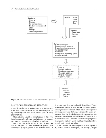
Source Solid
Excitation Liquid
Thermal Vapor
Plasma Gas
Ion bombardment
Electron bombardment
Laser
Voltage Transport
Chemical potential Gas phase
Vacuum
Liquid
Surface processes
Deposition of film specie
Deposition of contaminants
Ion bombardment
Desorption
Energy from depositing specie
External heating
Annealing
Inert atmosphere
Reactive atmosphere
Chemical reactions
Physical reactions
Global vs. local
Analysis
Physical
Chemical
Electrical
Optical
Figure 7.1 General features of thin film deposition processes
7.2 PVD-FILM GROWTH AND STRUCTURE is encountered in many epitaxial depositions. Three-
dimensional growth is also known as island growth.
Atoms impinging on a surface attach to the surface
Island growth is common when metals are deposited
either with chemical bonds (≈1 eV; chemisorption) or
by short-range van der Waals forces (≈0.3–0.4 eV; on insulators where the bonds between film atoms are
physisorption). stronger than the bonds between film atoms and the
These adatoms are able to move because of their own substrate. A third mode, called Stranski–Krastanov, is a
initial energy or by substrate-supplied energy or because mixture of 2D- and 3D-modes. Understanding of growth
they receive energy from the impinging particles. mechanisms is elusive and it is difficult to predict which
There are two main modes of film growth: 2D growth mode would take place.
and 3D (Figure 7.2). Two-dimensional growth, also If we measure the early stages of thin-film growth
called layer-by-layer growth, is the preferred mode. It by surface-sensitive techniques, for example, Auger