
Page 98 - Sami Franssila Introduction to Microfabrication
P. 98
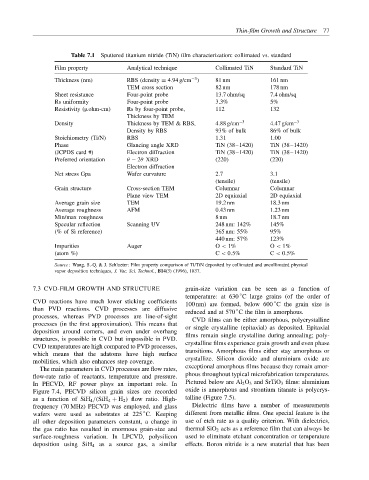
Thin-film Growth and Structure 77


                      Table 7.1  Sputtered titanium nitride (TiN) film characterization: collimated vs. standard
                 Film property        Analytical technique      Collimated TiN  Standard TiN
                                                         −3
                 Thickness (nm)       RBS (density = 4.94 g/cm )  81 nm        161 nm
                                      TEM cross section         82 nm          178 nm
                 Sheet resistance     Four-point probe          13.7 ohm/sq    7.4 ohm/sq
                 Rs uniformity        Four-point probe          3.3%           5%
                 Resistivity (µohm-cm)  Rs by four-point probe,  112           132
                                      Thickness by TEM
                 Density              Thickness by TEM & RBS,   4.88 g/cm −3   4.47 g/cm −3
                                      Density by RBS            93% of bulk    86% of bulk
                 Stoichiometry (Ti/N)  RBS                      1.31           1.00
                 Phase                Glancing angle XRD        TiN (38–1420)  TiN (38–1420)
                 (JCPDS card #)       Electron diffraction      TiN (38–1420)  TiN (38–1420)
                 Preferred orientation  θ − 2θ XRD              (220)          (220)
                                      Electron diffraction
                 Net stress Gpa       Wafer curvature           2.7            3.1
                                                                (tensile)      (tensile)
                 Grain structure      Cross-section TEM         Columnar       Columnar
                                      Plane view TEM            2D equiaxial   2D equiaxial
                 Average grain size   TEM                       19.2 nm        18.3 nm
                 Average roughness    AFM                       0.43 nm        1.23 nm
                 Min/max roughness                              8 nm           18.7 nm
                 Specular reflection   Scanning UV               248 nm: 142%   145%
                 (% of Si reference)                            365 nm: 55%    95%
                                                                440 nm: 57%    123%
                 Impurities           Auger                     O < 1%         O < 1%
                 (atom %)                                       C < 0.5%       C < 0.5%
                 Source: Wang, S.-Q. & J. Schlueter: Film property comparison of Ti/TiN deposited by collimated and uncollimated physical
                 vapor deposition techniques, J. Vac. Sci. Technol., B14(3) (1996), 1837.

           7.3 CVD-FILM GROWTH AND STRUCTURE           grain-size variation can be seen as a function of
                                                       temperature: at 630 C large grains (of the order of
                                                                       ◦
           CVD reactions have much lower sticking coefficients  100 nm) are formed, below 600 C the grain size is
                                                                                 ◦
           than PVD reactions. CVD processes are diffusive  reduced and at 570 C the film is amorphous.
                                                                      ◦
           processes, whereas PVD processes are line-of-sight  CVD films can be either amorphous, polycrystalline
           processes (in the first approximation). This means that  or single crystalline (epitaxial) as deposited. Epitaxial
           deposition around corners, and even under overhang  films remain single crystalline during annealing; poly-
           structures, is possible in CVD but impossible in PVD.
           CVD temperatures are high compared to PVD processes,  crystalline films experience grain growth and even phase
                                                       transitions. Amorphous films either stay amorphous or
           which means that the adatoms have high surface
                                                       crystallize. Silicon dioxide and aluminium oxide are
           mobilities, which also enhances step coverage.
             The main parameters in CVD processes are flow rates,  exceptional amorphous films because they remain amor-
           flow-rate ratio of reactants, temperature and pressure.  phous throughout typical microfabrication temperatures.
           In PECVD, RF power plays an important role. In  Pictured below are Al 2 O 3 and SrTiO 3 films: aluminium
           Figure 7.4, PECVD silicon grain sizes are recorded  oxide is amorphous and strontium titanate is polycrys-
           as a function of SiH 4 /(SiH 4 + H 2 ) flow ratio. High-  talline (Figure 7.5).
           frequency (70 MHz) PECVD was employed, and glass  Dielectric films have a number of measurements
           wafers were used as substrates at 225 C. Keeping  different from metallic films. One special feature is the
                                           ◦
           all other deposition parameters constant, a change in  use of etch rate as a quality criterion. With dielectrics,
           the gas ratio has resulted in enormous grain-size and  thermal SiO 2 acts as a reference film that can always be
           surface-roughness variation. In LPCVD, polysilicon  used to eliminate etchant concentration or temperature
           deposition using SiH 4 as a source gas, a similar  effects. Boron nitride is a new material that has been