
Page 99 - Sami Franssila Introduction to Microfabrication
P. 99
78 Introduction to Microfabrication
AFM:
Surface roughness
S = 40 nm S = 18 nm S = 17 nm S = 16 nm S = 4 anm
q
q
q
q
q
TEM:
Size and shape of the grains
25 nm
20 nm
20 nm
8 nm
750 nm
300 nm
200 nm 30 nm
1.25 2.5 5 7.5 8.6
(SiH ) / (SiH + H ) [%]
4
2
4
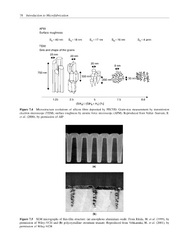
Figure 7.4 Microstructure evolutions of silicon films deposited by PECVD. Grain-size measurement by transmission
electron microscope (TEM); surface roughness by atomic force microscope (AFM). Reproduced from Vallat–Sauvain, E.
et al. (2000), by permission of AIP
(a)
(b)
Figure 7.5 SEM micrographs of thin-film structure: (a) amorphous aluminium oxide. From Ritala, M. et al. (1999), by
permission of Wiley-VCH and (b) polycrystalline strontium titanate. Reproduced from Vehkam¨ aki, M. et al. (2001), by
permission of Wiley-VCH