
Page 89 - Sami Franssila Introduction to Microfabrication
P. 89
68 Introduction to Microfabrication
Figure 6.4 Terrace step kink (TSK) growth model of epitaxy: growth proceeds at kinks, and atoms on flat surface diffuse
to energetically favourable positions at kinks. Wafer miscut creates terraced structure
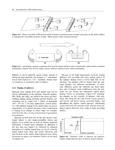
n +
p substrate
+
(a) (b)
Figure 6.5 Autodoping: dopants evaporated from heavily doped substrate add to intentionally added dopant (substrate
autodoping); dopants from heavily doped regions influence doping locally (lateral autodoping)
difficult. It can be aided by miscut wafers: instead of Because of the high temperatures involved, dopant
◦
slicing the ingot perfectly, for example, a 3 misorienta- diffusion will inevitably take place during epitaxy. If
tion is used (typical of <111> material). Atomic steps the epilayer doping level is lower than that of the
so created act as nucleation sites for epitaxy. substrate, the epilayer will be doped from the sub-
strate through two different mechanisms: (1) solid-
state diffusion across the substrate–epi layer inter-
6.2.1 Doping of epilayers
face and (2) dopant atom outdiffusion from the sub-
Epitaxial layer doping level and dopant type can be strate into gas stream and subsequent vapour phase
chosen independent of the substrate. Gaseous dopants, doping, known as autodoping (Figure 6.5). Autodop-
PH 3 , B 2 H 6 and AsH 3 , are added to the source gas flow, ing depends on the volatility of dopants, with anti-
enabling doping during epitaxial growth. Dopant con- mony (Sb) being the best (the lowest vapour pressure)
centration can be varied over 7 orders of magnitude and arsenic and boron having somewhat higher, and
−3
20
13
(10 –10 cm ). In many applications, several epilay- phosphorus the highest vapour pressure. Autodoping
ers with different doping levels and/or types are grown comes both from the substrate itself, and also from any
sequentially, or in graded structures where composition doped regions that have been made in steps preceding
or doping level changes in minor steps, for example, epitaxy.
from Si to Si 0.7 Ge 0.3 in tens of increments of germanium
concentration.
Epitaxial growth need not be the first process step: Transition width
doped silicon is also single-crystalline silicon and
epitaxy on it works just as well. In bipolar transistor
fabrication, a buried layer formation by diffusion is 50%
the first step (see Figure 3.2), followed by epitaxial Concentration
deposition of a lightly doped layer on top of a heavily
doped buried layer. Base and emitter diffusions will Epi layer
then be done in this lightly doped epitaxial layer. More Silicon substrate
discussion on epitaxy on structured wafers can be found Figure 6.6 Transition width at substrate–epi interface.
in Chapter 26. Lightly doped epitaxial layer on heavily doped substrate