
Page 88 - Sami Franssila Introduction to Microfabrication
P. 88
Epitaxy 67
less than 0.2%, and superlattices of AlAs/GaAs/AlAs 6
type can be grown easily, with periods down to atomic Deposition temperature,
2
layer thickness, equipment limitations allowing. 5 1270 °C H flow, one
liter/min
Heteroepitaxy for silicon materials is difficult because 4
no good lattice matching materials can be found. The
most important application is the growth of Si (1−x) Ge x 3
on silicon. The lattice constant of silicon is 5.43 ˚ A and Silicon deposition in microns/min 2
that of germanium is 5.66 ˚ A. The lattice constant of SiGe
alloys is described fairly well as a linear combination of 1
silicon and germanium lattice constants by 0
a Si (1−x) Ge x = (1 − x)a Si + xa Ge (6.1) −1
−2
There exists a critical thickness t c (which depends 0 0.1 0.2 0.3 0.4 0.5
on lattice constant and therefore germanium fraction) Mol fraction SiCl in H 2
4
below which mismatch can be accommodated by elastic
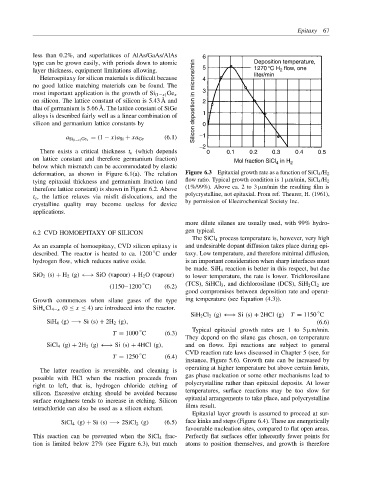
deformation, as shown in Figure 6.1(a). The relation Figure 6.3 Epitaxial growth rate as a function of SiCl 4 /H 2
tying epitaxial thickness and germanium fraction (and flow ratio. Typical growth condition is 1 µm/min, SiCl 4 /H 2
therefore lattice constant) is shown in Figure 6.2. Above (1%/99%). Above ca. 2 to 3 µm/min the resulting film is
t c , the lattice relaxes via misfit dislocations, and the polycrystalline, not epitaxial. From ref. Theurer, H. (1961),
crystalline quality may become useless for device by permission of Electrochemical Society Inc.
applications.
more dilute silanes are usually used, with 99% hydro-
6.2 CVD HOMOEPITAXY OF SILICON gen typical.
The SiCl 4 process temperature is, however, very high
As an example of homoepitaxy, CVD silicon epitaxy is and undesirable dopant diffusion takes place during epi-
◦
described. The reactor is heated to ca. 1200 C under taxy. Low temperature, and therefore minimal diffusion,
hydrogen flow, which reduces native oxide. is an important consideration when sharp interfaces must
be made. SiH 4 reaction is better in this respect, but due
SiO 2 (s) + H 2 (g) ←→ SiO (vapour) + H 2 O (vapour) to lower temperature, the rate is lower. Trichlorosilane
◦
(1150–1200 C) (6.2) (TCS), SiHCl 3 , and dichlorosilane (DCS), SiH 2 Cl 2 are
good compromises between deposition rate and operat-
Growth commences when silane gases of the type ing temperature (see Equation (4.3)).
SiH x Cl 4−x (0 ≤ x ≤ 4) are introduced into the reactor.
◦
SiH 2 Cl 2 (g) ←→ Si (s) + 2HCl (g) T = 1150 C
SiH 4 (g) −→ Si (s) + 2H 2 (g), (6.6)
◦
T = 1000 C (6.3) Typical epitaxial growth rates are 1 to 5 µm/min.
They depend on the silane gas chosen, on temperature
SiCl 4 (g) + 2H 2 (g) ←→ Si (s) + 4HCl (g), and on flows. Epi reactions are subject to general
CVD reaction rate laws discussed in Chapter 5 (see, for
◦
T = 1250 C (6.4)
instance, Figure 5.6). Growth rate can be increased by
operating at higher temperature but above certain limits,
The latter reaction is reversible, and cleaning is
gas phase nucleation or some other mechanisms lead to
possible with HCl when the reaction proceeds from
polycrystalline rather than epitaxial deposits. At lower
right to left, that is, hydrogen chloride etching of
temperatures, surface reactions may be too slow for
silicon. Excessive etching should be avoided because
epitaxial arrangements to take place, and polycrystalline
surface roughness tends to increase in etching. Silicon
films result.
tetrachloride can also be used as a silicon etchant.
Epitaxial layer growth is assumed to proceed at sur-
SiCl 4 (g) + Si (s) −→ 2SiCl 2 (g) (6.5) face kinks and steps (Figure 6.4). These are energetically
favourable nucleation sites, compared to flat open areas.
This reaction can be prevented when the SiCl 4 frac- Perfectly flat surfaces offer inherently fewer points for
tion is limited below 27% (see Figure 6.3), but much atoms to position themselves, and growth is therefore