
Page 87 - Sami Franssila Introduction to Microfabrication
P. 87
66 Introduction to Microfabrication
Epitaxy) and MBE, molecular beam epitaxy, are the two order of 1 µm/min, a factor of 100 higher. Typical
main epitaxy techniques. epi-poly thicknesses are 10 to 20 µm, compared with
The term epi-poly is used in micromechanics. It is 0.1 to 2 µm typical of LPCVD polysilicon, which is
self-contradictory: epitaxial films are single crystalline, used as a CMOS gate and surface micromechanics
and poly means polycrystalline. What is meant is structural layer.
that a CVD epireactor has been used to deposit a
thick layer of silicon, using epi growth conditions 6.1 HETEROEPITAXY
◦
(temperatures around 1100 C), but growth is on an
amorphous substrate, for example, SiO 2 , resulting in a Epitaxy on dissimilar materials is termed heteroepitaxy,
polycrystalline film. Standard polysilicon deposition in with examples such as AlAs on GaAs, GaN on SiC
◦
an LPCVD reactor at 630 C is a very slow process, or SiGe on Si. The Al x Ga 1−x As system is favourable
∼10 nm/min; whereas epitaxial growth rates are of the because lattice constants of all GaAs and AlAs differ by
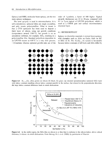
(a) (b)
Figure 6.1 Si (1−x) Ge x alloy grown on silicon (Si black, Ge gray): (a) strained (pseudomorphic) epitaxial SiGe layer
with lattice constant matching silicon lattice constant parallel to the surface, but relaxed in the perpendicular direction;
(b) large lattice constant difference leads to misfit dislocations
SiGe on Si (001)
10 4
People/bean: 550°C fit
Relaxed
Equilibrium theory (1)
Thickness t c ( Å) 10 3 Metastable (1): Bai et al. JAP 75 (1994) 4475
Pseudomorphic
Indications of relaxation
10 2
Stable
10 1
0 10 20 30 40 50 60 70 80 90 100
Ge fraction x (%)
Figure 6.2 In the stable region, the SiGe film on silicon is so thin that it conforms to the silicon lattice; above critical
thickness, it relaxes via misfit dislocations. From Herzog, H.-J. et al. (2000), by permission of Elsevier