
Page 84 - Sami Franssila Introduction to Microfabrication
P. 84
Thin-film Materials and Processes 63
(100–400 µV/K), and polysilicon is used in many ther- all the light impinging on it. Again, glass is a potential
moelectric devices. But CVD offers possibilities for substrate, but even cheaper substrates like steel or
realizing multilayer structures that cannot be made in polymers are being considered.
single-crystal materials. The Fabry–Perot interferome-
ter of Figure 1.8 utilizes two polysilicon layers, and
more functionality is built in by leaving some polysil- 5.11 SILICIDES
icon area undoped, which effectively results in insulat-
ing regions. A rather interesting class of conducting thin films is the
silicides: compounds of silicon and metal, for example,
TiSi 2 , CoSi 2 , NiSi, WSi 2 and PtSi. Silicides combine
5.11.1 Amorphous silicon
the good properties of silicon, such as high-temperature
PECVD of silicon from silane results in amorphous stability and metal-like resistivity, with the lowest values
silicon with a lot of embedded hydrogen. The film is of ca. 15 µohm-cm for resistivity (Table 5.8).
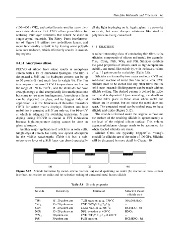
designated a-Si:H and its hydrogen content can be up Silicides are formed by two major methods: CVD and
to 30 atomic-% (and much less in weight %). The film solid-state reaction of metal thin film and silicon. CVD
is amorphous because PECVD temperatures are low, in silicides need to be etched like any other films, but the
◦
the range of 150 to 350 C, and the atoms do not have solid state–reacted silicide patterns can be made without
enough energy to find energetically favourable positions silicide etching. The desired pattern is defined in oxide,
but come to rest upon impingement. Amorphous silicon and metal is deposited. Upon annealing, metal–silicon
can be deposited on glass, and its biggest industrial reaction takes place in those areas where metal and
application is in the fabrication of thin-film transistors silicon are in contact, but on oxide the metal does not
(TFT) for active matrix displays. Electron and hole react. The unreacted metal can be etched away to leave
2
mobilities in annealed a-Si:H are only ca. 1 to 10 cm /V silicide and oxide (Figure 5.12).
s, which is adequate for switching transistors. In situ The silicide is formed under the original surface and
doping during PECVD is crucial in TFT fabrication the surface of the resulting silicide is approximately at
because high-temperature doping cannot be done on the level of the original silicon surface. This volume
glass substrates. expansion/thickness change needs to be accounted for
Another major application of a-Si:H is in solar cells. when reacted silicides are made.
◦
Single-crystal silicon has fairly low optical absorption Silicide CTEs are typically 15 ppm/ C. Young’s
in the visible wavelengths (Table 4.1) but a sub- moduli for silicides are of the order of 100 GPa. Silicides
micrometre layer of a-Si:H layer can absorb practically will be discussed in more detail in Chapter 19.
(a) (b) (c)
Figure 5.12 Silicide formation by metal–silicon reaction: (a) metal sputtering on wafer (b) reaction at metal–silicon
interface; no reaction on oxide and (c) selective etching of unreacted metal leaves silicide
Table 5.8 Silicide properties
Silicide Resistivity Formation Selective metal:
silicide etch
◦
TiSi 2 15–20 µohm-cm Ti/Si reaction at ca. 750 C NH 4 OH:H 2 O 2
TiSi 2 15–20 µohm-cm CVD TiCl 4 /SiH 2 Cl 2 /H 2 –
◦
CoSi 2 15–20 µohm-cm Co/Si reaction at 500 C HCl:H 2 O 2 3:1
◦
NiSi 15–20 µohm-cm Ni/Si reaction at 400 C HNO 3
◦
30 µohm-cm CVD WF 6 /SiH 2 Cl 2 at 400 C –
WSi 2
PtSi 30 µohm-cm Pt/Si reaction HCl:HNO 3 3:1