
Page 80 - Sami Franssila Introduction to Microfabrication
P. 80
Thin-film Materials and Processes 59
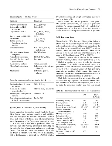
Structural parts of finished devices Densification anneal at a high temperature can lower
this by a factor of 2.
Function Examples Films should be free of pinholes, small point-
like defects; otherwise they are useless as protective
Inter-metal insulation SiO 2 , polymers 2
Gate oxides in MOS SiO 2 , HfO 2 coatings. For plasma-enhanced CVD, <0.1 pinholes/cm
transistors is a good value. If the film is less dense than the bulk, it
Capacitor dielectrics SiO 2 , Si 3 N 4 , Ta 2 O 5, can be either because of porosity or because of pinholes.
BaSrTiO 3
Tunnel oxide in EPROMs SiO 2 5.9.1 Inorganic films
Ion barriers Al 2 O 3 , Si 3 N 4
Tunnel oxides in AlO x , NbO x Thermal oxide, SiO 2 , is a very high quality dielectric
Josephson junction (Table 5.5), but it can only be grown on silicon (single or
devices polycrystalline silicon) and all the other materials on the
Dielectric mirrors CVD oxide, nitride, wafer have to be compatible with ca. 1000 C oxidizing
◦
polysilicon ambient, which excludes most materials. When silicon
Micromechanical beams LPCVD nitride dioxide is needed on materials other than silicon, it is
and plates done by CVD, either thermal CVD or PECVD.
Antireflective coatings PECVD SiN x , SiO 2 Thermally grown silicon dioxide is the standard
Heat sink for lasers and Diamond reference material, with its relative permittivity ε r of ca.
power devices 4 (dielectric constant ε = ε r ε 0 ). In order to minimize
Hydrophobic surfaces Teflon, diamond capacitances (C = εA/L) between metal layers, it is
Microfluidic structures Polymers, oxide, nitride, preferable to use low dielectric constant films (known
diamond as low-k or low-ε materials), many of them polymeric
Microlenses Polymers, spin-on materials, or modified CVD oxides. The topic of
glasses dielectric constant will be discussed in connection with
multilevel metallization for ICs in Chapter 27.
High dielectric–constant films are required in appli-
Protective coatings against ambient in final devices cations where high capacitance is needed. MOS transis-
tors and DRAM memories are capacitors, and in order
Passivation layer & metal SiO x , SiO x N y to make the capacitors smaller, area has been scaled
ion barrier
Humidity & scratch PECVD SiN x , polyimide
protecting barriers Table 5.5 Properties of silicon dioxide and silicon nitride
Tribological coating (wear, Diamond, SiC
SiO 2 Si 3 N 4
friction)
Corrosion resistant coatings Ta 2 O 5 , SiC (LPCVD)
in harsh environments Resistivity ( -cm), 25 C 10 16 10 16
◦
3
Density (g/cm ) 2.2 2.9–3.1
Dielectric constant 3.8–3.9 6–7
5.9 PROPERTIES OF DIELECTRIC FILMS Dielectric strength (V/cm) 12 × 10 6 10 × 10 6
Thermal expansion 0.5 1.6
◦
Higher deposition temperature usually leads to denser coefficient (ppm/ C)
◦
films that are more resistant to etching and polishing Melting point ( C) 1700 1800
and less susceptible to moisture absorption. Thermal Refractive index ◦ 1.46 2.00
oxide etch rate in hydrofluoric acid (HF) is always the Specific heat (J/g C) 1.0 0.7
same, irrespective of the furnace that was used to grow Young’s modulus (GPa) 87 ∼300
it. In CVD, and in PECVD in particular, films can Yield strength (GPa) 8.4 14
have HF etch rates varying enormously depending on Stress in film on Si (MPa) 200–400 C 1000 T
0.014
0.19
Thermal conductivity
the particular type of equipment and process conditions (W/cm K)
(power, flow rate and ratios, temperature). As a rule Etch rate in Buffered HF 100 1
of thumb, if thermal SiO 2 etch rate is 100 nm/min, (nm/min)
300 to 1000 nm/min is expected for (PE)CVD oxides.