
Page 75 - Sami Franssila Introduction to Microfabrication
P. 75
54 Introduction to Microfabrication
limitation due to deposition rates, which are gener- to be deposited by the electroless method. Gold can be
ally 1 to 100 nm/min. In many cases, thicker films are deposited from a KOH, KCN, KBH 4 and KAu(CN) 2
desired, and PVD or CVD methods quickly become mixture at rates exceeding 5 µm/min, even though
throughput limited. In CVD silicon epitaxy, a 100 µm much lower rates are usually used. Temperatures for
layer thickness is feasible, even though very expensive. electroless deposition range from room temperature to
◦
For most polycrystalline and amorphous CVD and PVD 100 C.
films, however, stresses build up to unacceptable levels Copper deposition chemistries traditionally use
for thicker films, limiting thicknesses to a few microme- sodium hydroxide in the plating bath, but this has to
tres. be eliminated if copper is used in IC metallization.
Liquid phase deposition methods include a wide vari- Alternative pH adjustment can be done with TMAH
ety of techniques that are unrelated physico-chemically. (tetramethyl ammonium hydroxide). Copper sulphate
Compared to PVD and CVD methods, liquid phase (CuSO 4 ) in formaldehyde (HCHO) and EDTA (ethylene
methods are extremely simple. A beaker is enough diamine tetraacetic acid) complexing agent are the
for electroless deposition (with an optional hot plate). basic constituents of the bath. Surfactants (polyethylene
′
Add a current source and an electroplating system is glygol) and stabilizers (2,2 -dipyridyl) can be added. The
ready. Liquid phase methods are widely used in printed reaction is described by
wiring board industry, thin-film head fabrication and in 2− −
MEMS, and they are being introduced in IC fabrication, CuEDTA + 2HCHO + 4OH −→
for deposition of copper and for inter-metal dielectric Cu + H 2 + 2H 2 O + 2HCOO + EDTA 4−
−
layer deposition.
◦
Liquid phase depositions take place at 20 to 100 C, The deposition rate is of the order of 100 nm/min. The
and film structure and quality are often very different electroless deposition set-up is extremely simple and no
from PVD and CVD films. But as is usual with other electrical connection needs to be made to the wafers.
deposition technologies, film properties will be strongly Selectivity, however, is difficult to maintain. Hydrogen
influenced by subsequent annealing steps. evolution and incorporation into the film is a problem
because hydrogen is mobile, and carbon incorporation is
another problem. With 2 µohm-cm as the accepted thin-
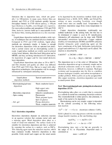
Liquid phase Typical applications film copper resistivity, electroless deposition can result
deposition methods in much poorer films.
- Electroplating/galvanic Thick conductor layers
deposition 5.6.2 Electroplating/galvanic plating/electrochemical
High aspect ratio deposition (ECD)
metallization
- Electroless deposition Selective metallization Electroplating takes place on a wafer that is connected
- Spin coating Photoresists as a cathode in metal-ion containing electrolyte solution.
Thick polymer layers The counterelectrode is either passive, like platinum, or
Spin-on-glasses made of the metal to be deposited.
- Sol–gel Porous dielectrics Electroplating can be very simple: copper is deposited
Thick, complex materials on the cathode according to the following reduc-
tion reaction:
−
Cu 2+ + 2e −→ Cu (s) electrolyte solution: CuSO 4
5.6.1 Electroless deposition
Gold is plated in a two-step process with the second, the
Electroless deposition depends on reduction reaction charge transfer reaction, as the rate-limiting step:
in an aqueous solution that contains metal salts and
−
a reducing agent. Metal deposition takes place as a Au(CN) 2 ←→ AuCN + CN −
result of metal ion reduction. The surface needs to be AuCN + e −→ Au (s) + CN −
−
suitable for electroless deposition and this is achieved
by exposing the surface to a catalyst, such as PdCl 2 . Electroplating rates vary a lot but are generally in
This reducing agent starts the reduction reaction, which the range of 0.1 to 10 µm/min. Deposited mass is
then continues locally. Selective deposition is thus calculated as
possible. Gold, nickel and copper are the usual metals mass = αItM /nF