
Page 74 - Sami Franssila Introduction to Microfabrication
P. 74
Thin-film Materials and Processes 53
Slope = E a2 400 kHz power
Surface Showerhead
Log rate Mass limited Electrode for gas
reaction
introduction
transport
limited Slope = E a1 Plasma
Wafer
High T Low T Heated electrode
(1/T)
Pumping system
Figure 5.6 Surface reaction–limited versus mass trans-
fer–limited CVD reactions
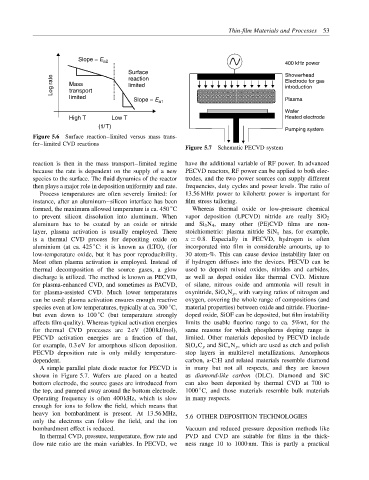
Figure 5.7 Schematic PECVD system
reaction is then in the mass transport–limited regime have the additional variable of RF power. In advanced
because the rate is dependent on the supply of a new PECVD reactors, RF power can be applied to both elec-
species to the surface. The fluid dynamics of the reactor trodes, and the two power sources can supply different
then plays a major role in deposition uniformity and rate. frequencies, duty cycles and power levels. The ratio of
Process temperatures are often severely limited: for 13.56 MHz power to kilohertz power is important for
instance, after an aluminum–silicon interface has been film stress tailoring.
◦
formed, the maximum allowed temperature is ca. 450 C Whereas thermal oxide or low-pressure chemical
to prevent silicon dissolution into aluminum. When vapor deposition (LPCVD) nitride are really SiO 2
aluminum has to be coated by an oxide or nitride and Si 3 N 4 , many other (PE)CVD films are non-
layer, plasma activation is usually employed. There stoichiometric: plasma nitride SiN x has, for example,
is a thermal CVD process for depositing oxide on x = 0.8. Especially in PECVD, hydrogen is often
◦
aluminium (at ca. 425 C: it is known as (LTO), (for incorporated into film in considerable amounts, up to
low-temperature oxide, but it has poor reproducibility. 30 atom-%. This can cause device instability later on
Most often plasma activation is employed. Instead of if hydrogen diffuses into the devices. PECVD can be
thermal decomposition of the source gases, a glow used to deposit mixed oxides, nitrides and carbides,
discharge is utilized. The method is known as PECVD, as well as doped oxides like thermal CVD. Mixture
for plasma-enhanced CVD, and sometimes as PACVD, of silane, nitrous oxide and ammonia will result in
for plasma-assisted CVD. Much lower temperatures oxynitride, SiO x N y , with varying ratios of nitrogen and
can be used: plasma activation ensures enough reactive oxygen, covering the whole range of compositions (and
◦
species even at low temperatures, typically at ca. 300 C, material properties) between oxide and nitride. Fluorine-
◦
but even down to 100 C (but temperature strongly doped oxide, SiOF can be deposited, but film instability
affects film quality). Whereas typical activation energies limits the usable fluorine range to ca. 5%wt, for the
for thermal CVD processes are 2 eV (200 kJ/mol), same reasons for which phosphorus doping range is
PECVD activation energies are a fraction of that, limited. Other materials deposited by PECVD include
for example, 0.3 eV for amorphous silicon deposition. SiO x C y and SiC x N y , which are used as etch and polish
PECVD deposition rate is only mildly temperature- stop layers in multilevel metallizations. Amorphous
dependent. carbon, a-C:H and related materials resemble diamond
A simple parallel plate diode reactor for PECVD is in many but not all respects, and they are known
shown in Figure 5.7. Wafers are placed on a heated as diamond-like carbon (DLC). Diamond and SiC
bottom electrode, the source gases are introduced from can also been deposited by thermal CVD at 700 to
◦
the top, and pumped away around the bottom electrode. 1000 C, and those materials resemble bulk materials
Operating frequency is often 400 kHz, which is slow in many respects.
enough for ions to follow the field, which means that
heavy ion bombardment is present. At 13.56 MHz, 5.6 OTHER DEPOSITION TECHNOLOGIES
only the electrons can follow the field, and the ion
bombardment effect is reduced. Vacuum and reduced pressure deposition methods like
In thermal CVD, pressure, temperature, flow rate and PVD and CVD are suitable for films in the thick-
flow rate ratio are the main variables. In PECVD, we ness range 10 to 1000 nm. This is partly a practical