
Page 51 - Sami Franssila Introduction to Microfabrication
P. 51
30 Introduction to Microfabrication
Gate
t = 25 nm
ox
1.5 nm
Source
Drain
n-type: 25 nm
19
2.0 × 10
19 y =
1.5 × 10 1.2 V
19
1.0 × 10 p-type
5 × 10 18 1.0 × 10 19 0.8 V
0
0.4 V
0
5 × 10 18
y = −0.4 V
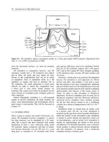
Figure 3.5 2D simulation: dopant concentration profiles of a 25 nm gate length CMOS transistor. Reproduced from
Taur, Y. et al. (1998), by permission of IEEE
from the horizontal surfaces, we need an atomistic grid spacing, 100 layers need to be calculated. Similar
simulator. grid size in 2D simulation requires 100 × 100 squares
6
4
2D simulation is computation intensive, and 2D (10 ), and in 3D it equals 10 cubes. Roughly speaking,
simulators usually have a 1D simulation tool embed- if 1D simulation takes seconds, 2D takes minutes and
ded in them, for quick and easy initial 1D tests. 3D, hours.
Saving on the computational time can be in orders However, a 10 nm grid is no good for 3D simulation
of magnitude. Grid, or simulation mesh, in a 1D because 3D simulation is used especially for 100 nm
simulator, is regular and easy to generate, but in devices and alike, and perhaps a 1 nm grid is used.
2D simulators, the mesh generation is much more But the question is not only computational; additional
difficult. In order to reduce the computation time, physical models need to be developed because more and
a dense grid is used where abrupt changes are more atomistic models must be used, and the continuum
expected, and a sparse grid where the gradients are not approximation fails because of the atomic nature of
steep. Instead of rectangular grids, triangular grids are matter. In order to take advantage of 3D-process
often employed. simulation, 3D-device simulators must be used, just as
Optical lithography simulation is a self-contained 2D-process simulators feed into 2D-device simulators.
regime in process simulation. Its main modules are Advanced device simulators must similarly account
optics, resist photochemistry and development, and its for the fact that electric current is not a continuous
main output is resist profile. This will be discussed in variable, but a stream of charge packets with 1.6 × 10 −19
Chapter 10. C charge.
Simulation needs to extend from an atomic scale
to a reactor scale. On the 1 m scale, simulation is
3.4 3D SIMULATION
needed to predict gas flows and temperature distributions
When scaling to smaller and smaller dimensions con- inside the reactor; on the micrometre scale, simulation
tinues, 3D simulation becomes mandatory. A narrow is needed to predict doping and deposition inside and
but long transistor can be simulated by a 2D simu- on microstructures, and an atomic level simulation is
lator, but a narrow and short transistor with similar needed for understanding the details of film growth
dimensions in both x- and y-directions really needs and diffusion. For thin-film deposition, such a simulator
3D treatment. Again, complexity and time of simula- would produce a relation between process parameters
tion increase drastically over the 2D case. If a 1 µm and film properties. At present, such a multiscale
deep layer is simulated in 1D simulator with 10 nm simulation remains a faraway goal.