
Page 52 - Sami Franssila Introduction to Microfabrication
P. 52
Simulation of Microfabrication Processes 31
0.0
−0.194
−0.388
−0.582
−0.776
−0.970
−1.164
−1.358
−1.552
−1.746
−1.940
0.0 0.306 0.613 0.920 1.227 1.534 1.841 2.148 2.455 2.762 3.069
(a)
(b)
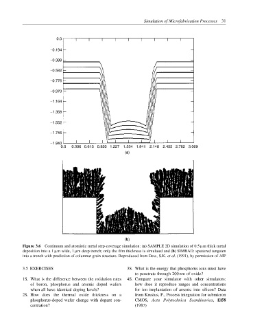
Figure 3.6 Continuum and atomistic metal step-coverage simulation: (a) SAMPLE 2D simulation of 0.5 µm thick metal
deposition into a 1 µm wide, 1 µm deep trench; only the film thickness is simulated and (b) SIMBAD: sputtered tungsten
into a trench with prediction of columnar grain structure. Reproduced from Dew, S.K. et al. (1991), by permission of AIP
3.5 EXERCISES 3S. What is the energy that phosphorus ions must have
to penetrate through 200 nm of oxide?
1S. What is the difference between the oxidation rates 4S. Compare your simulator with other simulators:
of boron, phosphorus and arsenic doped wafers how does it reproduce ranges and concentrations
when all have identical doping levels? for ion implantation of arsenic into silicon? Data
2S. How does the thermal oxide thickness on a from Krusius, P., Process integration for submicron
phosphorus-doped wafer change with dopant con- CMOS, Acta Polytechnica Scandinavica, El58
centration? (1987)