
Page 49 - Sami Franssila Introduction to Microfabrication
P. 49
28 Introduction to Microfabrication
Process simulation Over the years, more layers and more realistic mod-
-structures els have been added to 1D simulators, for instance,
-dopant profiles some simulators can handle the oxidation and doping of
-layer thicknesses
= = > input to device simulation polycrystalline silicon. Polycrystalline materials require
more inputs than single crystals, for example, grain size
Device simulation
-electrical, mechanical, thermal, optical behaviour and texture, and assumptions of grain boundary diffusion
-current-voltage, force-displacement, potential-flow versus bulk diffusion, among others. ICECREM (from
= = > input to circuit simulation Fraunhofer Institute FhG/IIS, Erlangen) is an advanced
Circuit simulation one-dimensional simulator. It can simulate the follow-
-output signal and noise ing processes:
-rise time, speed, delays
Figure 3.1 Levels of simulation
– epitaxy
– oxidation
and the device simulator results form the starting mate- – diffusion
rial for circuit simulation (Figure 3.1). – ion implantation
Circuit simulation is the most advanced and pro- – deposition of undoped oxide films (protective cap-
cess simulation is the least developed of the three ping layers)
kinds of simulations. Device simulators for CMOS today – deposition of doped oxide films (diffusion sources)
are predictive because CMOS device physics is well – etching (of oxide and silicon).
understood. Of course, continuous scaling to smaller
linewidths means that new phenomena must be imple-
mented into process and device simulators regularly. ICECREM models can account for a number of
important real life effects such as high phosphorus con-
centration in diffusion, implantation through oxide and
3.2 1D SIMULATION
oxidation enhanced diffusion (OED). These features will
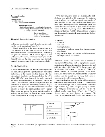
A one-dimensional simulator treats matter as layers, and be discussed in Chapters 13, 14 and 15. ICECREM
the simulation outputs are layer thicknesses and dopant output consists of diffusion profiles, oxide thick-
distributions in the vertical direction (Figure 3.2). One- nesses, sheet resistances and junction depths. Sensitivity
dimensional simulation has been used since the 1970s analysis can be carried out to study both process-
when SUPREM from Stanford University emerged. parameter and model-parameter changes.
Diffusion, ion implantation, oxidation and epitaxy are A typical simulator input file begins with the substrate
treated. Two additional, non-physical process steps are definition (crystal orientation 100 or 111, doping type
included: film deposition and etching, but these are just and level/resistivity). Grid is defined next: simulation
geometrical steps, like ‘add 500 nm of undoped oxide on depth is fixed (e.g. 5 µm, and grid spacing is defined
silicon’, or ‘remove the top 50 nm of silicon by etching’. (e.g. 0.01 µm). Concentrations that need to be cal-
15
21
−3
These steps are needed for more realistic models of culated usually range from 10 cm −3 to 10 cm .
surfaces and interfaces, but they do not reveal anything Process steps are then defined in sequence, fol-
about the deposition or etching processes. lowed by output commands. Model parameters can be
n emitter
+
p base
n epi
+
n buried layer
p substrate
Figure 3.2 Cross section of an npn-bipolar transistor and its 1D simulation model of dopant concentrations along the
cut line