
Page 44 - Sami Franssila Introduction to Microfabrication
P. 44
Micrometrology and Materials Characterization 23
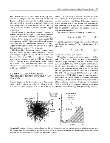
back towards the surface, slows down on the way back, matter. The scattering of electrons spreads the beam
and finally emerges from the solid and reaches the to a volume much larger than the beam spot on the
detector. All these steps can be handled calculation- surface, as shown in the Figure 2.12. Auger electrons,
ally, since RBS is a quantitative method. Elastic recoil which originate at the very surface, are unaffected by
from heavy atoms is more pronounced, and RBS is this spreading, but X-rays and backscattered electrons
ideally suited for atoms like arsenic, tantalum, copper that are generated deep inside the sample can escape
or tungsten. and reach the detector.
Signal energy is sometimes confusing because it The radius of X-ray signals can be estimated by
depends not only on the depth at which it originates but
also on the mass of the atom that caused backscattering. R x (µm) = 0.04 V 1.75 /ρ (2.9)
In Figure 2.11, a tantalum barrier beneath copper has
been measured by RBS. Silicon signal is weak because
where the acceleration voltage is given in kilovolts and
silicon is a light atom and beneath copper and tantalum. the density in grams/cm . The analysis radius R is
3
Copper is the topmost layer, but because it is lighter given by
than tantalum, its peak is lower in energy.
2
RBS detectability depends on matrix: elements lighter R = R + d 2 (2.10)
x
than the matrix are not readily detectable. Oxygen
and nitrogen analysis on top of silicon wafers are where d is the beam spot diameter.
therefore difficult for RBS. Mass separation between This radius of electron microprobe analysis (EMPA)
neighbouring elements is poor in RBS, and therefore (a.k.a. EDX or energy dispersive X-ray analysis) can be
silicon, aluminium and phosphorous cannot readily orders of magnitude bigger than the electron beam spot
be resolved. The RBS-detection limits are around size. EMPA/EDX can detect elemental concentrations
20
−3
10 cm , but with heavy elements, it even goes down at 1% level. Examples of suitable analytical tasks
17
to 10 cm −3 (0.001%). include phosphorous determination in doped oxide
(5% wt typical) or copper concentration in aluminium
film (0.5–4% Cu typical). EMPA/EDX is most often
2.11 EMPA (ELECTRON MICROPROBE
ANALYSIS)/EDX (ENERGY DISPERSIVE X-RAY connected to a SEM, which is used to image the area of
ANALYSIS) interest first, and then subjected to elemental analysis by
EMPA/EDX. If the sample is made thin, of the order of
Electron beams can be focussed down to 5 nm spots, 100 nm, electron scattering effects can be eliminated.
and the devices can be probed for localized analysis. This is utilized in transmission electron microscopy
The electron beam diverges as it interacts with the (TEM) and electron energy loss spectroscopy (EELS).
E o Low-energy Higher-energy
secondary inelastically
electrons scattered
Backscattered electrons
electrons
Escape 0−50 eV
depth
0 Energy E o
Figure 2.12 A finely focussed electron beam hits the sample surface, and low-energy secondary electrons escape from
the surface only, but backscattered and inelastically scattered electrons contribute to signals deep inside the sample.
Reproduced from Schaffner, T.J. (2000), by permission of IEEE