
Page 39 - Sami Franssila Introduction to Microfabrication
P. 39
18 Introduction to Microfabrication
(a) (b)
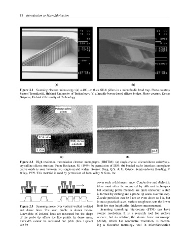
Figure 2.1 Scanning electron microscopy: (a) a 400 µm thick SU-8 pillars in a microfluidic bead trap. Photo courtesy
Santeri Tuomikoski, Helsinki University of Technology; (b) a heavily boron-doped silicon bridge. Photo courtesy Kestas
Grigoras, Helsinki University of Technology
Polycrystalline
silicon
27 Å oxide
(100) silicon
substrate
3.13 Å 50 Å
(a) (b)
Figure 2.2 High-resolution transmission electron micrographs (HRTEM): (a) single-crystal silicon/silicon oxide/poly-
crystalline silicon structure. From Buchanan, M. (1999), by permission of IBM; (b) bonded wafer interface: amorphous
native oxide is seen between two single-crystal wafers. Source: Tong, Q.Y. & U. G¨ osele, Semiconductor Bonding,
Wiley, 1999. This material is used by permission of John Wiley & Sons, Inc
cover such a thickness range. Conductive and dielectric
films must often be measured by different techniques
but scanning probe methods are quite universal: a step
is formed by etching and a probe-tip scans over the step.
Z-scale precision can be 1 nm or even down to 1 ˚ A, but
in most practical cases, surface roughness sets the lower
Figure 2.3 Scanning probe over vertical walled, isolated limit for step height/film thickness measurement.
and dense lines. The scan profile is shown below. Scanning tunnelling microscope (STM) can have
Linewidths of isolated lines are measured but the shape atomic resolution. It is a research tool for surface
of the probe tip affects the line profile. In dense array, science, but its relative, the atomic force microscope
linewidth cannot be measured but pitch (line + space) (AFM), which has nanometre resolution, is becom-
can be ing a favourite metrology tool in microfabrication