
Page 42 - Sami Franssila Introduction to Microfabrication
P. 42
Micrometrology and Materials Characterization 21
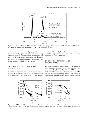
b (002)
bcc (110)
Intensity (a.u.) Ta/TaNx = 158/5(nm)
Tantalum on TaNx
R = 0.97 Ω/
s
b (202) Tantalum on SiO 2
b (410) bcc (110) Ta = 144 (nm)
R = 10.5 Ω/
s
30 35 40 45 50
2 q (deg)
Figure 2.8 X-ray diffraction of tantalum thin films: the underlying material has a major effect on film crystal structure
and resistivity. Reproduced from Ohmi, T. (2001), by permission of IEEE
the initial state: amorphous and polycrystalline silicon atomic identification by X-ray fluorescence, that is, char-
behave differently upon subsequent annealing. X-ray acteristic X-ray radiation. TXRF can measure surface
−2
10
diffraction provides structural information (Figure 2.8). impurities at a level of 10 cm .
TEM also provides similar information, but TEM anal-
ysis area is in tens of nanometres, whereas XRD gives
an average over hundreds of micrometres. 2.7 SIMS (SECONDARY ION MASS
SPECTROMETRY)
2.6 TXRF (TOTAL REFLECTION X-RAY In SIMS, the surface to be analysed is bombarded by
FLUORESCENCE) ions that detach secondary ions. These secondary ions
are mass-analysed, giving their identity. SIMS is thus a
If minute amounts of matter on wafer surface must be surface-sensitive technique, but another important SIMS
analysed, total reflection can be used. A method known application is depth profiling: the ion beam erodes the
as total reflection X-ray fluorescence (TXRF) provides surface, and layers beneath the surface become available
10 22 10 22
Concentration (cm −3 ) 10 20 5 keV Concentration (cm −3 ) 10 20 5 keV
21
21
10
10
1 keV
19
19
10
10
18
18
10
10
1 keV
10
16
16
10 17 10 17
10
0 200 400 600 800 0 200 400 600 800
Depth (Å) Depth (Å)
(a) (b)
Figure 2.9 SIMS data of low-energy arsenic implantation into silicon with two different energies: (a) immediately after
implantation; (b) after 1050 C, 10 s heat treatment. Reproduced from Plummer, J.D. & P.B. Griffin (2001), by permission
◦
of IEEE