
Page 41 - Sami Franssila Introduction to Microfabrication
P. 41
20 Introduction to Microfabrication
When the sample size is 15 times larger than the wafer fab measurements can thus be discarded after
probe spacing, resistivity is correct within 1%. For the fabrication is completed. This saves area because
smaller samples, geometric correction factors need to the dicing saw requires a margin of ca. one hundred
be applied. micrometres between the chips anyway, as shown in
Thickness has to be measured independently. Alterna- Figure 1.13.
tively, sheet resistance can be used to calculate thickness
after thin-film resistivity is known (bulk values cannot
usually be used). 2.4 PHYSICAL AND CHEMICAL ANALYSES
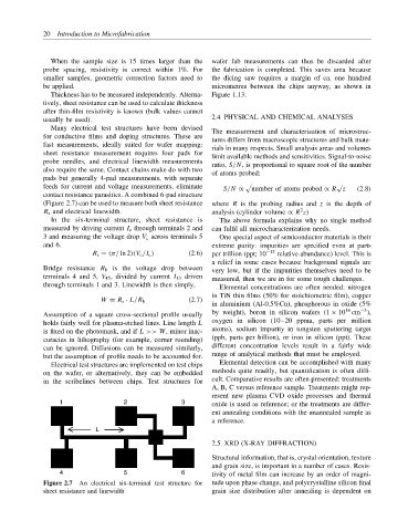
Many electrical test structures have been devised The measurement and characterization of microstruc-
for conductive films and doping structures. These are tures differs from macroscopic structures and bulk mate-
fast measurements, ideally suited for wafer mapping: rials in many respects. Small analysis areas and volumes
sheet resistance measurement requires four pads for limit available methods and sensitivities. Signal-to-noise
probe needles, and electrical linewidth measurements
ratio, S/N, is proportional to square root of the number
also require the same. Contact chains make do with two
of atoms probed:
pads but generally 4-pad measurements, with separate
feeds for current and voltage measurements, eliminate √
S/N ∝ number of atoms probed ∝ R z (2.8)
contact resistance parasitics. A combined 6-pad structure
(Figure 2.7) can be used to measure both sheet resistance where R is the probing radius and z is the depth of
2
R s and electrical linewidth. analysis (cylinder volume ∝ R z)
In the six-terminal structure, sheet resistance is The above formula explains why no single method
measured by driving current I c through terminals 2 and can fulfil all microcharacterization needs.
3 and measuring the voltage drop V c across terminals 5 One special aspect of semiconductor materials is their
and 6. extreme purity: impurities are specified even at parts
R s = (π/ ln 2)(V c /I c ) (2.6) per trillion (ppt; 10 −12 relative abundance) level. This is
a relief in some cases because background signals are
Bridge resistance R b is the voltage drop between
very low, but if the impurities themselves need to be
terminals 4 and 5, V 45 , divided by current I 13 driven measured, then we are in for some tough challenges.
through terminals 1 and 3. Linewidth is then simply, Elemental concentrations are often needed: nitrogen
in TiN thin films (50% for stoichiometric film), copper
W = R s · L/R b (2.7)
in aluminium (Al-0.5%Cu), phosphorous in oxide (5%
−3
16
Assumption of a square cross-sectional profile usually by weight), boron in silicon wafers (1 × 10 cm ),
holds fairly well for plasma-etched lines. Line length L oxygen in silicon (10–20 ppma, parts per million
atoms), sodium impurity in tungsten sputtering target
is fixed on the photomask, and if L >> W, minor inac-
(ppb, parts per billion), or iron in silicon (ppt). These
curacies in lithography (for example, corner rounding)
different concentration levels result in a fairly wide
can be ignored. Diffusions can be measured similarly,
but the assumption of profile needs to be accounted for. range of analytical methods that must be employed.
Electrical test structures are implemented on test chips Elemental detection can be accomplished with many
on the wafer, or alternatively, they can be embedded methods quite readily, but quantification is often diffi-
in the scribelines between chips. Test structures for cult. Comparative results are often presented: treatments
A, B, C versus reference sample. Treatments might rep-
resent new plasma CVD oxide processes and thermal
1 2 3 oxide is used as reference; or the treatments are differ-
ent annealing conditions with the unannealed sample as
a reference.
L
2.5 XRD (X-RAY DIFFRACTION)
Structural information, that is, crystal orientation, texture
and grain size, is important in a number of cases. Resis-
4 5 6 tivity of metal film can increase by an order of magni-
Figure 2.7 An electrical six-terminal test structure for tude upon phase change, and polycrystalline silicon final
sheet resistance and linewidth grain size distribution after annealing is dependent on