
Page 40 - Sami Franssila Introduction to Microfabrication
P. 40
Micrometrology and Materials Characterization 19
L
W T
Figure 2.5 Conceptualizing metal line as a number of
four square elements: R = 4R s
a rectangular piece of conducting material, resistance is
given by
R = ρL/WT (2.1)
where ρ is resistivity, L, length, T , thickness and W,
width (Figure 2.5).
If we consider a square piece of metal, L = W, we
can then define sheet resistance, R s ,
R s ≡ ρ/T (2.2)
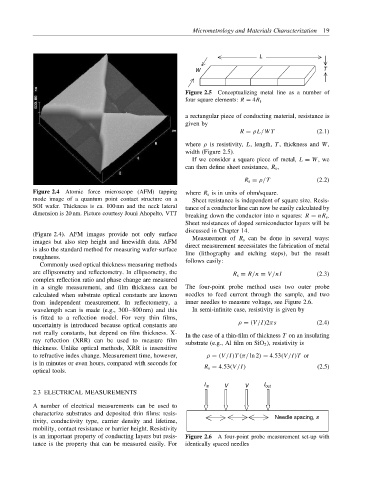
Figure 2.4 Atomic force microscope (AFM) tapping where R s is in units of ohm/square.
mode image of a quantum point contact structure on a Sheet resistance is independent of square size. Resis-
SOI wafer. Thickness is ca. 100 nm and the neck lateral tance of a conductor line can now be easily calculated by
dimension is 20 nm. Picture courtesy Jouni Ahopelto, VTT
breaking down the conductor into n squares: R = nR s .
Sheet resistances of doped semiconductor layers will be
discussed in Chapter 14.
(Figure 2.4). AFM images provide not only surface Measurement of R s can be done in several ways:
images but also step height and linewidth data. AFM direct measurement necessitates the fabrication of metal
is also the standard method for measuring wafer-surface line (lithography and etching steps), but the result
roughness. follows easily:
Commonly used optical thickness measuring methods
are ellipsometry and reflectometry. In ellipsometry, the R s = R/n = V/nI (2.3)
complex reflection ratio and phase change are measured
in a single measurement, and film thickness can be The four-point probe method uses two outer probe
calculated when substrate optical constants are known needles to feed current through the sample, and two
from independent measurement. In reflectometry, a inner needles to measure voltage, see Figure 2.6.
wavelength scan is made (e.g., 300–800 nm) and this In semi-infinite case, resistivity is given by
is fitted to a reflection model. For very thin films,
uncertainty is introduced because optical constants are ρ = (V/I)2πs (2.4)
not really constants, but depend on film thickness. X- In the case of a thin-film of thickness T on an insulating
ray reflection (XRR) can be used to measure film substrate (e.g., Al film on SiO 2 ), resistivity is
thickness. Unlike optical methods, XRR is insensitive
to refractive index change. Measurement time, however, ρ = (V/I)T (π/ ln 2) = 4.53(V/I)T or
is in minutes or even hours, compared with seconds for R s = 4.53(V/I) (2.5)
optical tools.
I in V V I out
2.3 ELECTRICAL MEASUREMENTS
A number of electrical measurements can be used to
characterize substrates and deposited thin films: resis- Needle spacing, s
tivity, conductivity type, carrier density and lifetime,
mobility, contact resistance or barrier height. Resistivity
is an important property of conducting layers but resis- Figure 2.6 A four-point probe measurement set-up with
tance is the property that can be measured easily. For identically spaced needles