
Page 43 - Sami Franssila Introduction to Microfabrication
P. 43
22 Introduction to Microfabrication
for analysis. When the erosion rate is known, SIMS data sensitive technique. Auger can identify surface atoms,
provides information about atomic concentrations as a be they residues from previous steps or contaminants
function of depth. from processes. Auger is therefore a tool for surface
SIMS measurement is slow and expensive, but it chemical analysis (Figure 2.10).
is the accepted standard for dopant depth distribution With the aid of sample erosion technique (similar to
measurement (even though we are most often interested SIMS), Auger can be transformed into a depth-profiling
in electrically active dopants, whereas SIMS only counts technique: after surface analysis, sputtering removes
atoms). SIMS offers nanometre depth resolution and 10 6 some material, and the Auger measurement of the newly
dynamic range (Figure 2.9). formed surface is made. This is continued until the
desired sample depth is probed.
2.8 AUGER ELECTRON SPECTROSCOPY (AES)
2.9 XPS (X-RAY PHOTOELECTRON
In Auger measurement an electron beam (3–5 keV) SPECTROSCOPY)/ESCA
hits the surface, and an inner core electron is ejected.
An electron from an outer shell fills the hole, and The X-ray photoelectron spectroscopy (XPS) is closely
gives off excess energy during transition. Another outer related to Auger in two senses: low-energy electrons are
shell electron receives this energy and escapes. The analysed, and because their escape depth is so small,
energy of this Auger electron is uniquely determined the method is surface-sensitive, but XPS excitation
by the atomic structure, and therefore the identity of the is by X-rays. This has an important ramification for
element giving rise to the signal can be determined. The the analysis area: X-ray spots are fairly large, in the
escape depth of low energy Auger electrons is of the hundred micrometre range, and large areas are needed
order of nanometer, which makes Auger a truly surface for analysis.
Primary X-rays (a few kilovolts) eject electrons from
the sample. The energy of ejected electrons is related to
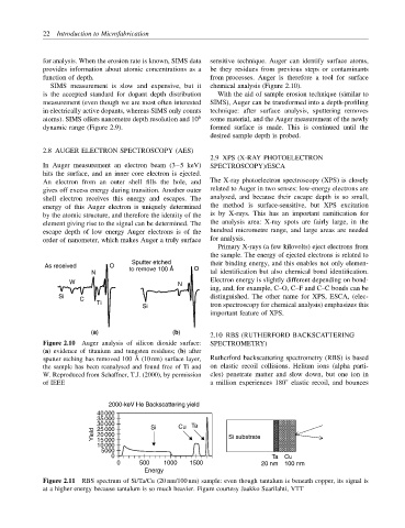
Sputter etched their binding energy, and this enables not only elemen-
As received O to remove 100 Å O
N tal identification but also chemical bond identification.
W N Electron energy is slightly different depending on bond-
ing, and, for example, C–O, C–F and C–C bonds can be
Si C distinguished. The other name for XPS, ESCA, (elec-
Ti
Si tron spectroscopy for chemical analysis) emphasizes this
important feature of XPS.
(a) (b)
2.10 RBS (RUTHERFORD BACKSCATTERING
Figure 2.10 Auger analysis of silicon dioxide surface: SPECTROMETRY)
(a) evidence of titanium and tungsten residues; (b) after
sputter etching has removed 100 ˚ A (10 nm) surface layer, Rutherford backscattering spectrometry (RBS) is based
the sample has been reanalysed and found free of Ti and on elastic recoil collisions. Helium ions (alpha parti-
W. Reproduced from Schaffner, T.J. (2000), by permission cles) penetrate matter and slow down, but one ion in
of IEEE a million experiences 180 elastic recoil, and bounces
◦
2000-keV He Backscattering yield
40 000
35 000
30 000 Si Cu Ta
25 000
Yield 20 000 Si substrate
15 000
10 000
5000
0 Ta Cu
0 500 1000 1500 20 nm 100 nm
Energy
Figure 2.11 RBS spectrum of Si/Ta/Cu (20 nm/100 nm) sample: even though tantalum is beneath copper, its signal is
at a higher energy because tantalum is so much heavier. Figure courtesy Jaakko Saarilahti, VTT