
Page 35 - Sami Franssila Introduction to Microfabrication
P. 35
14 Introduction to Microfabrication
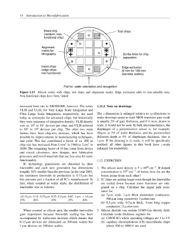
Inked chip Test chips
(random, non-
functional chip)
Alignment
marks for
lithography Scribe lines for chip
separation
Inked chips Edge exclusion
(edge chips (6 mm for 100-mm
non-functional) diameter wafers)
Flat for wafer orientation and recognition
Figure 1.13 Silicon wafer with chips, test chips and alignment marks. Edge exclusion adds to non-saleable area.
Non-functional chips have been ‘inked’
increased form one to 100 000 000, however. The terms 1.11.1 Note on drawings
VLSI and ULSI, for Very Large Scale Integration and
Ultra Large Scale Integration, respectively, are used The z-dimension is enlarged relative to xy-directions to
today as synonyms for advanced chips, but historically make drawings easier to read. MOS transistor gate oxide
they were measures of integration density: VLSI density is usually 2% of gate thickness, and if it were drawn to
5
7
was ca. 10 to 10 devices per chip, and ULSI referred scale, it would not be seen. In bulk micromechanics, the
7
9
to 10 to 10 devices per chip. The other two main diaphragm of a piezoresistive sensor is, for example,
factors have been chip-size increase, which has been 20 µm, or 5% of wafer thickness, and the piezoresistor
possible by improvements in manufacturing techniques, diffusion depth is 5% of diaphragm thickness, that is
and yield. This has contributed a factor of ca. 200 as 1 µm. If the drawing is to scale, it will be specifically
2
2
chip size has increased from 1 mm in 1960 to 2 cm in notified; all other figures in this book have z-scale
2000. The remaining factor of 10 has come from device enlarged for readability.
and circuit cleverness: new designs, new fabrication
processes and novel materials that use less area for same
functionality. 1.12 EXERCISES
IC technology generations are classified by their
−3
22
linewidths and each new generation has dimensions 1. The silicon atom density is 5 × 10 cm . If dopant
15
roughly 30% smaller than the previous. In the year 2003, concentration is 10 cm −3 of boron, how far are the
the minimum linewidth in production is 0.13 µm but boron atoms from each other?
this presents just a fraction of all IC’s manufactured. In 2. IC chips are getting larger even though the linewidths
fact, when counted as wafer starts, the distribution of are scaled down because more functions are inte-
linewidths was as follows: grated on a chip. Calculate the signal path resis-
tance for
(a) 3 µm wide, 1 µm thick aluminium conductors,
≤0.13 µm 0.18–0.25 µm 0.35–0.5 µm 0.65–1 µm >1.0 µm
15% 20% 20% 15% 30% 500 µm long (resistivity 3 µohm-cm)
(b) 0.3 µm wide, 0.5 µm thick, 1 mm long copper
conductors (2 µohm-cm)
When counted as silicon area, the smaller linewidths 3. Silicon dioxide can sustain 10 MV/cm electric field.
gain importance because linewidth scaling has been Calculate oxide thickness regimes for
accompanied by wafer-size increase which means that (a) CMOS ICs where operating voltages are 1 to 5 V
0.13 µm devices are fabricated on 300 mm wafers but (b) capillary electrophoresis (CE) microfluidic chips
1 µm devices on 100 mm wafers. where 500 to 5000 V are used