
Page 31 - Sami Franssila Introduction to Microfabrication
P. 31
10 Introduction to Microfabrication
the substrate is not machined or modified. Thin-film
transistors (TFTs) are most often fabricated on non-
semiconductor substrates: glass, plastic or steel. Surface
micromechanical devices like switches, relays, DNA
arrays, fluidic channels and gas sensors are often
fabricated on silicon wafers for convenience but they
could be fabricated on glass substrates as well.
1.8.4 Membrane devices
Membrane devices are a sub-class of thin-film devices:
Figure 1.7 Surface devices: a 0.5 µm CMOS in a scan-
ning electron microscope view again, all functionality is in the thin top layer, but
instead of full wafer mechanical support, only a thin
membrane supports the structures. Many thermal devices
In silicon CMOS (Figure 1.7), only the top 5 µm are membrane devices for thermal isolation: thermopiles,
layer of the wafer is used in making the active device, bolometers, chemical microreactors and mass flow
and the remaining 500 µm of wafer thickness is for meters (Figure 1.9). Many acoustic devices also utilize
support: mechanical strength and impurity control. Sur- bulk removal. Optical paths can be opened by removing
face devices can have very elaborate three-dimensional the bulk semiconductor. X-ray lithography masks are
structures, like multilevel metallization in logic circuits, gold or tungsten microstructures on a micrometre-
which can be 10 µm thick but this is still only a frac- thick membrane.
tion of wafer thickness; therefore the term surface device
applies.
1.8.5 Stacked devices
1.8.3 Thin-film devices Stacked devices are made by layer transfer and bonding
techniques. Two or more wafers are joined together per-
Devices can be built by depositing and patterning thin manently. Devices with vacuum cavities, for example,
films on the wafers, and the wafer has no role in device absolute pressure sensors, accelerometers and gyro-
operation. Wafer properties like thermal conductivity scopes are stacked devices made of bonded sili-
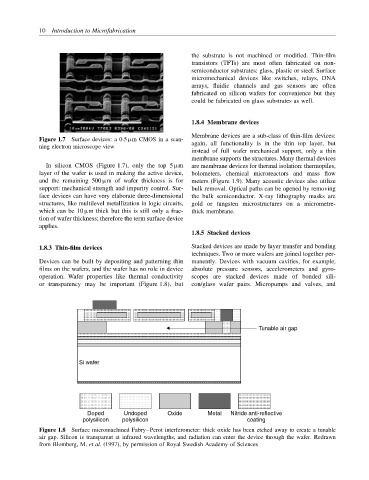
or transparency may be important (Figure 1.8), but con/glass wafer pairs. Micropumps and valves, and
Tunable air gap
Si wafer
Doped Undoped Oxide Metal Nitride anti-reflective
polysilicon polysilicon coating
Figure 1.8 Surface micromachined Fabry–Perot interferometer: thick oxide has been etched away to create a tunable
air gap. Silicon is transparent at infrared wavelengths, and radiation can enter the device through the wafer. Redrawn
from Blomberg, M. et al. (1997), by permission of Royal Swedish Academy of Sciences