
Page 26 - Sami Franssila Introduction to Microfabrication
P. 26
Introduction 5
films experience grain growth, for instance, during Surface
heat treatments; amorphous films can stay amorphous Film 2
or they can crystallize, usually into polycrystalline Interface 2 Film 1
state and under very special circumstances into single- Interface 1 Substrate
crystalline state.
Elemental substrates and elemental thin films are sim-
ple and they have various uses; silicon, aluminium, Figure 1.2 Materials and interfaces in a schematic
copper and tungsten are widely used. Compounds intro- microstructure
duce new possibilities and challenges: silicon dioxide
(SiO 2 ), silicon nitride (Si 3 N 4 ), hafnium dioxide (HfO 2 ),
Surface physical properties like roughness and reflec-
titanium silicide (TiSi 2 ), titanium nitride (TiN) and alu-
tivity are material and fabrication process dependent.
minium nitride (AlN) are not necessarily stoichiometric
The chemical nature of the surface is equally impor-
when deposited. For instance, titanium nitride is more
tant: many surfaces are covered by native oxide films
accurately described as TiN x , with the exact value of x
(e.g., silicon, aluminium and titanium form surface
determined by the details of the deposition process.
oxides readily) and by residual films. Adsorbed gases
In addition to elemental and compound materials,
and moisture affect processing via adhesion or nucle-
alloys are widely used. Instead of using elemental alu-
ation changes.
minium for metallization, it is beneficial to use Al–1% Si
Thick substrates are not immune to thin films: a thin
or Al–0.5% Si–2% Cu alloy, for metallization stability,
film of a few tens of nanometres may have such a high
as will be seen in Chapter 24. Alloys of dissimilar-sized
stress that a 500 µm thick silicon wafer is curved; or
atoms often result in amorphous films, and in some minute iron contamination on the surface will diffuse
applications, it is beneficial to maintain amorphousness
through a 500 µm thick wafer during a fairly moderate
upon annealing and to prevent crystallization. thermal treatment.
Deposition conditions strongly affect thin-film prop-
erties, for example via impurity incorporation or pro-
cess temperature: silicon will be amorphous if deposited 1.5 PROCESSES
at low temperature, polycrystalline at medium temper-
atures and single-crystalline material can be obtained Microfabrication processes consist of four basic
at high temperatures under tightly controlled condi- operations:
tions. Materials in microfabrication must be amenable to
micropatterning technologies, which translates to either 1. High-temperature processes
etching or polishing. Sometimes it is enough to deposit 2. Thin-film deposition processes
films on flat, planar wafers, but most often the films have 3. Patterning
to extend over steps and into trenches, which may be 40 4. Layer transfer and bonding.
times deeper than wide. These severe topographies intro-
duce further deposition process–dependent subtleties. Surface preparation and wafer cleaning could be termed
the fifth basic operation but unlike the four others,
wafer cleaning is never done in isolation: it is always
1.4 SURFACES AND INTERFACES closely connected with both the preceding and the
following process steps. Under each basic operation,
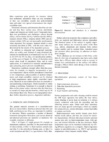
The general material structure of a microfabricated there are many specific technologies, which are suitable
device is shown below. Interfaces between thin-film and for certain devices, certain substrates, certain linewidths
bulk, and between two films, are important for stability or certain cost levels.
of structures. Wafers experience a number of thermal High-temperature steps modify dopant atom distri-
treatments during their fabrication, and various chemical butions inside silicon, and they are crucial for transis-
and physical processes are operative at interfaces: for tor characteristics. Devices like piezo-resistive pressure
example, reactions or diffusion. sensors also rely on high-temperature steps, with epi-
Film 1 of Figure 1.2 might present for example an taxy and resistor diffusion as the key processes. High-
aluminium conductor, and film 2 is the passivation layer temperature steps can be simulated extensively, by solv-
of silicon nitride, or film 1 is flash-memory tunnel oxide ing diffusion equations on a computer. High-temperature
◦
and film 2 is the polysilicon floating gate, or film 1 is regime in microfabrication is ca. 900 C and upwards,
oxide insulation and film 2 is a gas-sensitive SnO 2 film. temperatures where dopants readily diffuse.