
Page 28 - Sami Franssila Introduction to Microfabrication
P. 28
Introduction 7
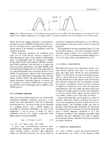
3.5 eV
2.2 eV
◦
Figure 1.4 Diffusion process: 2.2 eV barrier can be crossed at ease at 900 C but the frequency of crossing the 3.5 eV
◦
barrier is low. Higher temperature, for example, 1050 C, would be needed for the 3.5 eV barrier to be crossed at ease
fluidic devices for channel enclosure, in microelectro- exponential temperature dependencies, as are diffusion,
mechanical systems (MEMS) bonding forms sealed cav- electromigration and grain growth (which are physical
ities for resonating devices, and bonding enables single- processes).
crystal silicon to be attached on amorphous oxide for The magnitude of the pre-exponential factor z(T ) and
electrical insulation. the activation energy E a vary a lot. In etching reactions,
These elementary operations are combined many activation energy is below 1 eV, in polysilicon deposi-
times over to create devices. Process complexity is tion E a is 1.7 eV, in substitutional dopant diffusion it is
often discussed in terms of the number of lithography 3.5 to 4 eV and in silicon self-diffusion it is 5 eV.
steps: six lithography steps are enough for a simple
P-Type Metal-Oxide Semiconductor (PMOS) transistor
(late 1960s technology, and still used as a student lab 1.6 LATERAL DIMENSIONS
process in many universities), and many MEMS, solar
cell and flat-panel display devices can be made with two Microfabricated systems have dimensions around 1 µm:
to six photolithography steps even today but the 0.18 µm some devices perform well with 5 or 10 µm struc-
tures, and others need 100 nm for good performance
CMOS (Complementary Metal Oxide Semiconductor)
(Figure 1.5). But almost every device includes structures
circuits of year 2000 need 25 lithography steps. Systems
with ca. 100 µm dimension. These are needed to inter-
which combine CMOS with other functionalities, like
face the microdevices to the outside world: most devices
bipolar transistors, integrated displays or sensors, use
need electrical connections (by wire bonding or bump-
for example, 0.5 to 0.8 µm CMOS with 15 mask levels,
ing process); microfluidic devices must be connected
and add half a dozen lithography steps in addition to the
to capillaries or liquid reservoirs; solar cells and power
CMOS process.
semiconductors must have thick and large metal areas
to bring out the high currents involved, and connections
1.5.1 Arrhenius behaviour to and from optical fibres require structures about the
size of fibres, which is also of the order of 100 µm.
Many chemical and physical processes are exponentially Narrow individual lines can be made by a variety of
temperature dependent. Arrhenius equation is a very methods; what really counts is resolution; the power to
general and useful description of the rates of thermally resolve two neighboring structures. It determines device-
activated processes. Activation energy can be illustrated packing density. The resolution usually gets most of
as a jumping process over a barrier (Figure 1.4). attention when microscopic dimensions are discussed,
According to Boltzman distribution, an atom at the but alignment between structures in different lithography
temperature T has an excess of energy E a with a steps is equally important. Alignment is, as a rule
probability exp(−E a /kT ). Higher temperature leads of thumb, one-third of the minimum linewidth. High
higher barrier crossing probability resolution but poor alignment can result in inferior
device-packing density compared with poorer resolution
rate = z(T ) exp(−E a /kT ) (1.1) but tighter alignment.
k = 1.38 × 10 −23 J/K or 8.62 × 10 −5 eV/K.
A great many microfabrication processes show 1.7 VERTICAL DIMENSIONS
Arrhenius-type dependence: etching, resist develop-
ment, oxidation, epitaxy, chemical vapor deposition As a rule of thumb, vertical and lateral dimensions
(which are chemical processes) are all governed by of microdevices are similar. If the height-to-width,