
Page 32 - Sami Franssila Introduction to Microfabrication
P. 32
Introduction 11
many micropower devices like turbines and thrusters are
stacked devices with up to six wafers bonded together
(Figure 1.10). More and more layer transfer and wafer
bonding techniques are being developed, and stacked
devices of various sorts are expected to appear; for
example, GaAs optical devices bonded to Si-based elec-
tronics, or MEMS devices bonded to ICs.
1.9 MOS TRANSISTOR
The metal-oxide-semiconductor transistor, MOS, has
been the driving force of microfabrication industries.
It is the number one device by all measures: number
of devices sold, silicon area consumed, the narrowest
linewidths and the thinnest oxides in mass production, as
Figure 1.9 Mass flow sensor: a resonating bridge over
an etched channel. Reproduced from Bouwstra, S. et al. well as dollar value of production. Most equipment for
(1990), by permission of Elsevier microfabrication have originally been designed for MOS
IC fabrication, and later adapted to other applications.
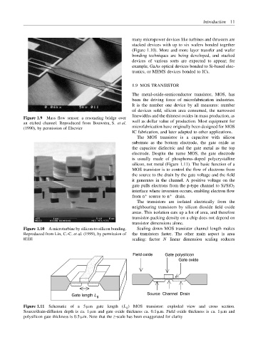
The MOS transistor is a capacitor with silicon
substrate as the bottom electrode, the gate oxide as
the capacitor dielectric and the gate metal as the top
electrode. Despite the name MOS, the gate electrode
is usually made of phosphorus-doped polycrystalline
silicon, not metal (Figure 1.11). The basic function of a
MOS transistor is to control the flow of electrons from
the source to the drain by the gate voltage and the field
it generates in the channel. A positive voltage on the
gate pulls electrons from the p-type channel to Si/SiO 2
interface where inversion occurs, enabling electron flow
+
from n source to n + drain.
The transistors are isolated electrically from the
neighbouring transistors by silicon dioxide field oxide
areas. This isolation eats up a lot of area, and therefore
transistor-packing density on a chip does not depend on
transistor dimensions alone.
Figure 1.10 A microturbine by silicon-to-silicon bonding. Scaling down MOS transistor channel length makes
Reproduced from Lin, C.-C. et al. (1999), by permission of the transistors faster. The other main aspect is area
IEEE scaling: factor N linear dimension scaling reduces
Field oxide Gate polysilicon
Gate oxide
Gate length L g Source Channel Drain
Figure 1.11 Schematic of a 5 µm gate length (L g ) MOS transistor: exploded view and cross section.
Source/drain-diffusion depth is ca. 1 µm and gate oxide thickness ca. 0.1 µm. Field oxide thickness is ca. 1 µm and
polysilicon gate thickness is 0.5 µm. Note that the z-scale has been exaggerated for clarity