
Page 27 - Sami Franssila Introduction to Microfabrication
P. 27
6 Introduction to Microfabrication
Low-temperature processes leave metal-to-silicon wafers and other substrates; by definition they are layers
◦
interface stable, and generally, 450 C is regarded as the deposited on top of a substrate. Thin-film steps do not
upper limit for low temperatures. In between 450 and affect dopant distribution inside silicon, that is, diodes
◦
900 C, there is a middle range that must be discussed and transistors are unaffected by them.
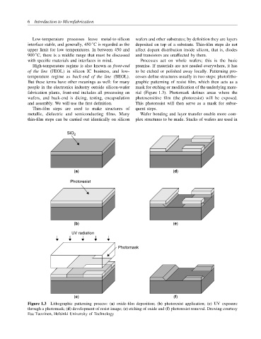
with specific materials and interfaces in mind. Processes act on whole wafers; this is the basic
High-temperature regime is also known as front-end premise. If materials are not needed everywhere, it has
of the line (FEOL) in silicon IC business, and low- to be etched or polished away locally. Patterning pro-
temperature regime as back-end of the line (BEOL). cesses define structures usually in two steps: photolitho-
But these terms have other meanings as well: for many graphic patterning of resist film, which then acts as a
people in the electronics industry outside silicon-wafer mask for etching or modification of the underlying mate-
fabrication plants, front-end includes all processing on rial (Figure 1.3). Photomask defines areas where the
wafers, and back-end is dicing, testing, encapsulation photosensitive film (the photoresist) will be exposed.
and assembly. We will use the first definition. This photoresist will then serve as a mask for subse-
Thin-film steps are used to make structures of quent steps.
metallic, dielectric and semiconducting films. Many Wafer bonding and layer transfer enable more com-
thin-film steps can be carried out identically on silicon plex structures to be made. Stacks of wafers are used in
SiO 2
(a) (d)
Photoresist
(b) (e)
UV radiation
Photomask
(c) (f)
Figure 1.3 Lithographic patterning process: (a) oxide-film deposition; (b) photoresist application; (c) UV exposure
through a photomask; (d) development of resist image; (e) etching of oxide and (f) photoresist removal. Drawing courtesy
Esa Tuovinen, Helsinki University of Technology