
Page 30 - Sami Franssila Introduction to Microfabrication
P. 30
Introduction 9
Finger ‘Inverted’ pyramids
p +
n + n Oxide
p-silicon
p +
p + p +
Rear contact Oxide
(a)
Half
cell
Width Cell space
(L )
(L ) s
w
Source Gate Source
n + n +
R CH R ACC R ACC R CH
p p
p + R JFET p +
R epl
n −
n +
Drain
(b)
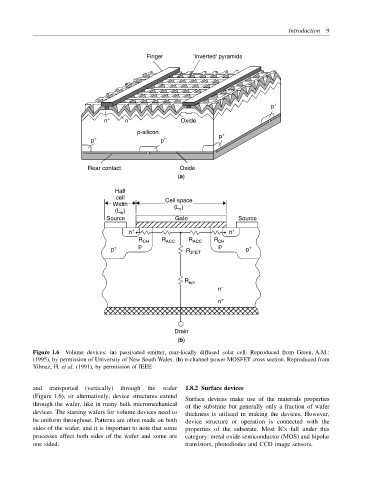
Figure 1.6 Volume devices: (a) passivated emitter, rear-locally diffused solar cell. Reproduced from Green, A.M.:
(1995), by permission of University of New South Wales. (b) n-channel power MOSFET cross section. Reproduced from
Yilmaz, H. et al. (1991), by permission of IEEE
and transported (vertically) through the wafer 1.8.2 Surface devices
(Figure 1.6), or alternatively, device structures extend
Surface devices make use of the materials properties
through the wafer, like in many bulk micromechanical
of the substrate but generally only a fraction of wafer
devices. The starting wafers for volume devices need to thickness is utilized in making the devices. However,
be uniform throughout. Patterns are often made on both device structure or operation is connected with the
sides of the wafer, and it is important to note that some properties of the substrate. Most ICs fall under this
processes affect both sides of the wafer and some are category: metal oxide semiconductor (MOS) and bipolar
one sided. transistors, photodiodes and CCD image sensors.