
Page 25 - Sami Franssila Introduction to Microfabrication
P. 25
4 Introduction to Microfabrication
Electrons in semiconductors + ⇒ Microelectronics
M
I
Photons in semiconductors + ⇒ Optoelectronics
C
R
Instrumentation + O ⇒ Micromechanics
F
A
Chemistry & biotechnology + B ⇒ Microfluidics
R
Optics + I ⇒ Micro-optics
C
A
Quantum mechanics + T ⇒ Nanotechnology
I
Robotics/mechatronics + O ⇒ Micromachines
N
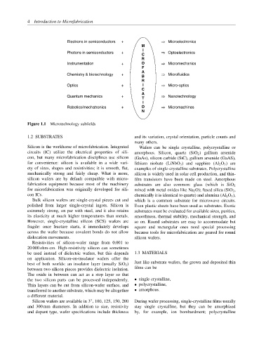
Figure 1.1 Microtechnology subfields
1.2 SUBSTRATES and its variation, crystal orientation, particle counts and
many others.
Silicon is the workhorse of microfabrication. Integrated Wafers can be single crystalline, polycrystalline or
circuits (IC) utilize the electrical properties of sili- amorphous. Silicon, quartz (SiO 2 ) gallium arsenide
con, but many microfabrication disciplines use silicon (GaAs), silicon carbide (SiC), gallium arsenide (GaAS),
for convenience: silicon is available in a wide vari- lithium niobate (LiNbO 3 ) and sapphire (Al 2 O 3 ) are
ety of sizes, shapes and resistivities; it is smooth, flat, examples of single-crystalline substrates. Polycrystalline
mechanically strong and fairly cheap. What is more, silicon is widely used in solar cell production, and thin-
silicon wafers are by default compatible with micro- film transistors have been made on steel. Amorphous
fabrication equipment because most of the machinery substrates are also common: glass (which is SiO 2
for microfabrication was originally developed for sili- mixed with metal oxides like Na 2 O); fused silica (SiO 2 ,
con ICs. chemically it is identical to quartz) and alumina (Al 2 O 3 ),
Bulk silicon wafers are single-crystal pieces cut and which is a common substrate for microwave circuits.
polished from larger single-crystal ingots. Silicon is Even plastic sheets have been used as substrates. Exotic
extremely strong, on par with steel, and it also retains substrates must be evaluated for available sizes, purities,
its elasticity at much higher temperatures than metals. smoothness, thermal stability, mechanical strength, and
However, single-crystalline silicon (SCS) wafers are so on. Round substrates are easy to accommodate but
fragile: once fracture starts, it immediately develops square and rectangular ones need special processing
across the wafer because covalent bonds do not allow because tools for microfabrication are geared for round
dislocation movements. silicon wafers.
Resistivities of silicon-wafer range from 0.001 to
20 000 ohm-cm. High-resistivity silicon can sometimes
be used instead of dielectric wafers, but this depends 1.3 MATERIALS
on application. Silicon-on-insulator wafers offer the
best of both worlds: an insulator layer (usually SiO 2 ) Just like substrate wafers, the grown and deposited thin
between two silicon pieces provides dielectric isolation. films can be
The oxide in between can act as a stop layer so that
the two silicon parts can be processed independently. • single crystalline,
Thin layers can be cut from silicon-wafer surface, and • polycrystalline,
transferred to another substrate, which may be altogether • amorphous.
a different material.
′′
Silicon wafers are available in 3 , 100, 125, 150, 200 During wafer processing, single-crystalline films usually
and 300 mm diameters. In addition to size, resistivity stay single crystalline, but they can be amorphized
and dopant type, wafer specifications include thickness by, for example, ion bombardment; polycrystalline