
Page 29 - Sami Franssila Introduction to Microfabrication
P. 29
8 Introduction to Microfabrication
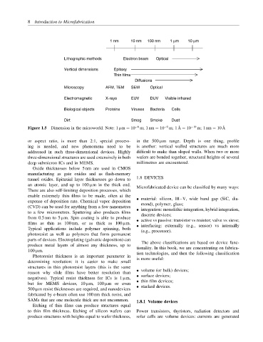
1 nm 10 nm 100 nm 1 µm 10 µm
Lithographic methods Electron beam Optical
Vertical dimensions Epitaxy
Thin films
Diffusions
Microscopy AFM, TEM SEM Optical
Electromagnetic X-rays EUV DUV Visible infrared
Biological objects Proteins Viruses Bacteria Cells
Dirt Smog Smoke Dust
Figure 1.5 Dimension in the microworld. Note: 1 µm = 10 −6 m; 1 nm = 10 −9 m; 1 ˚ A = 10 −10 m; 1 nm = 10 ˚ A
or aspect ratio, is more than 2:1, special process- in the 500 µm range. Depth is one thing, profile
ing is needed, and new phenomena need to be is another: vertical walled structures are much more
addressed in such three-dimensional devices. Highly difficult to make than sloped walls. When two or more
three-dimensional structures are used extensively in both wafers are bonded together, structural heights of several
deep submicron ICs and in MEMS. millimetres are encountered.
Oxide thicknesses below 5 nm are used in CMOS
manufacturing as gate oxides and as flash-memory
tunnel oxides. Epitaxial layer thicknesses go down to 1.8 DEVICES
an atomic layer, and up to 100 µm in the thick end.
Microfabricated device can be classified by many ways:
There are also self-limiting deposition processes, which
enable extremely thin films to be made, often at the • material: silicon, III–V, wide band gap (SiC, dia-
expense of deposition rate. Chemical vapor deposition mond), polymer, glass;
(CVD) can be used for anything from a few nanometres • integration: monolithic integration, hybrid integration,
to a few micrometres. Sputtering also produces films discrete devices;
from 0.5 nm to 5 µm. Spin coating is able to produce
• active vs passive: transistor vs resistor; valve vs sieve;
films as thin as 100 nm, or as thick as 100 µm.
• interfacing: externally (e.g., sensor) vs internally
Typical applications include polymer spinning, both (e.g., processor).
photoresist as well as polymers that form permanent
parts of devices. Electroplating (galvanic deposition) can
produce metal layers of almost any thickness, up to The above classifications are based on device func-
100 µm. tionality. In this book, we are concentrating on fabrica-
tion technologies, and then the following classification
Photoresist thickness is an important parameter in
is more useful:
determining resolution: it is easier to make small
structures in thin photoresist layers (this is the same
reason why slide films have better resolution than • volume (or bulk) devices;
negatives). Typical resist thickness for ICs is 1 µm, • surface devices;
but for MEMS devices, 10 µm, 100 µm or even • thin film devices;
• stacked devices.
500 µm resist thicknesses are required, and nanodevices
fabricated by e-beam often use 100 nm thick resist, and
SAMs that are one molecule thick are not uncommon. 1.8.1 Volume devices
Etching of thin films can produce structures equal
to thin film thickness. Etching of silicon wafers can Power transistors, thyristors, radiation detectors and
produce structures with heights equal to wafer thickness, solar cells are volume devices: currents are generated