
Page 151 - MEMS and Microstructures in Aerospace Applications
P. 151
Osiander / MEMS and microstructures in Aerospace applications DK3181_c007 Final Proof page 140 1.9.2005 12:04pm
140 MEMS and Microstructures in Aerospace Applications
Moving plate Spring
AR coating
Silicon
dioxide
Multilayer Conductive
dielectric Optical gap epoxy
Capacitor Electrical
plates lead Bonding pad
Silicon nitride
Silicon
Stationary plate
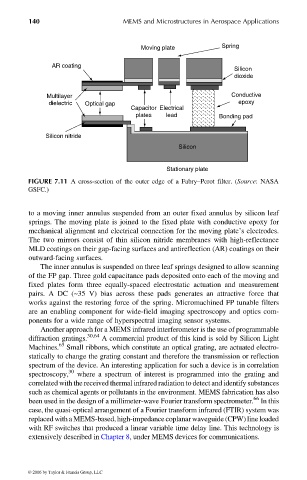
FIGURE 7.11 A cross-section of the outer edge of a Fabry–Perot filter. (Source: NASA
GSFC.)
to a moving inner annulus suspended from an outer fixed annulus by silicon leaf
springs. The moving plate is joined to the fixed plate with conductive epoxy for
mechanical alignment and electrical connection for the moving plate’s electrodes.
The two mirrors consist of thin silicon nitride membranes with high-reflectance
MLD coatings on their gap-facing surfaces and antireflection (AR) coatings on their
outward-facing surfaces.
The inner annulus is suspended on three leaf springs designed to allow scanning
of the FP gap. Three gold capacitance pads deposited onto each of the moving and
fixed plates form three equally-spaced electrostatic actuation and measurement
pairs. A DC (~35 V) bias across these pads generates an attractive force that
works against the restoring force of the spring. Micromachined FP tunable filters
are an enabling component for wide-field imaging spectroscopy and optics com-
ponents for a wide range of hyperspectral imaging sensor systems.
Another approach for a MEMS infrared interferometer is the use of programmable
30,64
diffraction gratings. A commercial product of this kind is sold by Silicon Light
65
Machines. Small ribbons, which constitute an optical grating, are actuated electro-
statically to change the grating constant and therefore the transmission or reflection
spectrum of the device. An interesting application for such a device is in correlation
spectroscopy, 30 where a spectrum of interest is programmed into the grating and
correlated with the received thermal infrared radiation to detect and identify substances
such as chemical agents or pollutants in the environment. MEMS fabrication has also
66
been used in the design of a millimeter-wave Fourier transform spectrometer. In this
case, the quasi-optical arrangement of a Fourier transform infrared (FTIR) system was
replaced with a MEMS-based, high-impedance coplanarwaveguide (CPW)line loaded
with RF switches that produced a linear variable time delay line. This technology is
extensively described in Chapter 8, under MEMS devices for communications.
© 2006 by Taylor & Francis Group, LLC