
Page 293 - MEMS and Microstructures in Aerospace Applications
P. 293
Osiander / MEMS and microstructures in Aerospace applications DK3181_c012 Final Proof page 285 1.9.2005 9:13pm
MEMS Packaging for Space Applications 285
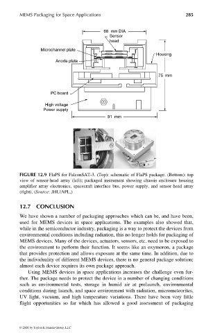
68 mm DIA
Sensor
head
Microchannel plate
Housing
Anode plate
75 mm
PC board
High voltage
Power supply
91 mm
FIGURE 12.9 FlaPS for FalconSAT-3. (Top): schematic of FlaPS package. (Bottom): top
view of sensor-head array (left); packaged instrument showing chassis enclosure housing
amplifier array electronics, spacecraft interface bus, power supply, and sensor-head array
(right). (Source: JHU/APL.)
12.7 CONCLUSION
We have shown a number of packaging approaches which can be, and have been,
used for MEMS devices in space applications. The examples also showed that,
while in the semiconductor industry, packaging is a way to protect the devices from
environmental conditions including radiation, this no longer holds for packaging of
MEMS devices. Many of the devices, actuators, sensors, etc. need to be exposed to
the environment to perform their function. It seems like an oxymoron, a package
that provides protection and allows exposure at the same time. In addition, due to
the individuality of different MEMS devices, there is no general package solution;
almost each device requires its own package approach.
Using MEMS devices in space applications increases the challenge even fur-
ther. The package needs to protect the device in a number of changing conditions
such as environmental tests, storage in humid air at prelaunch, environmental
conditions during launch, and space environment with radiation, micrometeorites,
UV light, vacuum, and high temperature variations. There have been very little
flight opportunities so far which has allowed a good assessment of packaging
© 2006 by Taylor & Francis Group, LLC