
Page 290 - MEMS and Microstructures in Aerospace Applications
P. 290
Osiander / MEMS and microstructures in Aerospace applications DK3181_c012 Final Proof page 282 1.9.2005 9:13pm
282 MEMS and Microstructures in Aerospace Applications
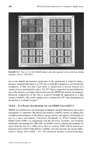
FIGURE 12.7 Sets of six VEC-MEMS shutter array die attached to the aluminum nitride
substrate. (Source: JHU/APL.)
test or the launch environment, protection of this instrument is achieved using a
polymer commercially known as CP1 that is both IR transmissive and electrically
conductive. A film, less than 4-mm thick, is sandwiched in tension between two
window frames and bonded in place. The CP1 film is suspended several millimeters
above the shutters, providing a barrier between the MEMS die and the environment.
Electrical conductivity of the film is achieved through the application of a thin
coating of InSnO 2 . This oxide coating serves to protect the CP1 from degradation in
the presence of atomic oxygen. 12
12.6.2 FLAT PLASMA SPECTROMETER FOR THE USAFA FALCONSAT-3
MEMS microfabrication and packaging techniques enabled fabrication and system
integration of a miniature flat plasma spectrometer (FlaPS) capable of making fine
resolution measurements of the kinetic energy spectra and angular distributions of
ions in a space environment. Conceived conceptually by NASA Goddard Space
Flight Center (GSFC) in conjunction with the Air Force Academy, and designed,
fabricated, and packaged by JHU/APL, the FlaPS reduces a plasma spectrometer for
space from the size of a coffee-urn to that of a teacup. FlaPs will be placed as a
payload on the USAFA FalconSAT-3 satellite, and will measure ion spectra differ-
ential in energy with a DE/E ~ 5%. The instrument includes a sensor-head array,
© 2006 by Taylor & Francis Group, LLC